background image

– 10 –

4-2.

ADJ  MODE

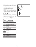
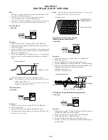
The following operations are performed in the ADJ mode, which
is set by connecting the TP1 (ADJ : JW98) terminal to the Ground
and turning on the power.

• During playback, there is no problem even if the GFS is continu-

ously LOW.

• High speed search is prohibited during access.
• During playback, the gain of focus servo and spindle servo does

not decrease.

• Servo related manual operations and measurement can be

performed.
(For details of operations, refer to Table of Key Operrations in
ADJ Mode.)

4-3.

CLV-S  MODE

The spindle servo for playback sets into the CLV-S mode when
the TP2 (AFADJ) terminal is connected to Ground after turning on
the power.

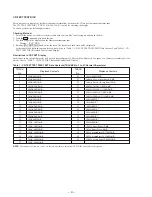
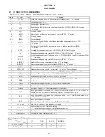
TABLE  OF  BUTTON  OPERATIONS  IN  ADJ  MODE

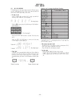
The jitter value display mode can be set after the all-music
remaining number mode using the 

[TIME/TEXT]

 button.

The functions of the number buttons are shown in the following
table.

FUNCTIONS  OF  NUMBER  BUTTONS
(With the attached remote commander)

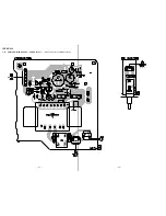
[ MAIN  BOARD ]  – Conductor Side –

Button

Function

1

Focus bias up

2

Focus bias aliasing (upper, middle, lower) display

3

Focus bias (best point, jitter value) display

4

Tracking servo, sled servo off

5

Tracking gain up

6

Focus bias down

7

Focus bias readjustment

8

Focus bias 00 point

9

Tracking servo, sled servo on

10

Tracking gain normal

11

S-Curve mode (play mode only)

12

Eccentric mode

13

14

Reserved for BD

15

16

17

Tracking gain initialize

18

Offset display (TE), EF, Bias

19

Offset display (VC, FE, RF)

20

Auto gain (FCS, TRK)

CLR key

(Error Rate, RFCK, GFS) selection

IC930

JW096

TP2
(AFADJ)

TP1
(ADJ)

JW098

IC302

CN302

Содержание CDP-XB820

Страница 1: ...RVICE MANUAL COMPACT DISC PLAYER AEP Model Model Name Using Similar Mechanism NEW CD Mechanism Type CDM36 14E Base Unit Type BU 14E Optical Pick up Type KSS 213B F NP SPECIFICATIONS CDP XB820 Continued on next page ...

Страница 2: ...CK UP MOTOR Section 24 6 7 Printed Wiring Board MAIN Section 25 6 8 Schematic Diagram MAIN Section 1 2 27 6 9 Schematic Diagram MAIN Section 2 2 29 6 10 Printed Wiring Boards POWER Section 31 6 11 Schematic Diagram POWER Section 33 6 12 Printed Wiring Boards PANEL Section 35 6 13 Schematic Diagram PANEL Section 37 7 EXPLODED VIEWS 42 8 ELECTRICAL PARTS LIST 46 SAFETY RELATED COMPONENT WARNING COMP...

Страница 3: ...sconnected chip component Notice that the minus side of a tantalum capacitor may be dam aged by heat NOTES ON HANDLING THE OPTICAL PICK UP BLOCK OR BASE UNIT CAUTION Use of controls or adjustments or performance of procedures other than those specified herein may result in hazardous ra diation exposure This appliance is classified as a CLASS 1 LASER product The CLASS 1 LASER PRODUCT MARKING is loc...

Страница 4: ...ng it For details refer to Table 2 CD TEXT DISC Recorded Contents and Display Table 1 CD TEXT TEST DISC TEXT Data Contents TRACKS No 1 to 41 Normal Characters 1 1kHz 0dB L R 22 1kHz 90dB L R 2 20Hz 0dB L R 23 Infinity Zero w o emphasis L R 3 40Hz 0dB L R 24 Infinity Zero with emphasis L R 4 100Hz 0dB L R 25 400Hz 7kHz 4 1 0dB L R 5 200Hz 0dB L R 26 400Hz 7kHz 4 1 10dB L R 6 500Hz 0dB L R 27 19kHz ...

Страница 5: ... 3Fh A B C D E F G 40h to 47Fh H I J K L M N O 48h to 4Fh P Q R S T U VW 50h to 57Fh X Y Z _ 58h to 5Fh a b c d e f g 60h to 67Fh h i j k l m n o 68h to 6Fh p q r s t u v w 70h to 77Fh x y z I 78h to 7Fh i A0h to A7h 8859 1 C ª PR A8h to AFh 2 3 µ B0h to B7h 1 º B8h to BFh À Á Â Ã Ä ÅÆÇ C0h to C7Fh È É Ê Ë Ì Í Î Ï C8h to CFh D Ñ Ò Ó Ô Õ Ö D0h to D7Fh Ø Ù Ú Û Ü Y ß D8h to DFh à á â ã ä å æ ç E0h to...

Страница 6: ...tton 5 TIME TEXT button 6 Remote sensor 7 0 button 8 button 9 EDIT TIME FADER button 0 CHECK button CLEAR button Fluorescent indicator tube PHONES jack PHONE LEVEL knob FILTER knob PEAK SEARCH button AUTO SPACE button MUSIC SCAN button ª LANGUAGE button º Disc tray OPEN CLOSE button button P button p button AMS PUSH ENTER knob ...

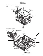
Страница 7: ...SECTION 2 two screws case 3TP2 2 two screws case 3TP2 3 case 1 two screws BV RING 2 two screws case 3TP2 3 loading panel ass y 2 two claws A 1 Push the slide cam in the direction of the arrow A 4 connector CN903 5 connector CN351 6 flat wire 25 core CN302 8 claw 7 five screws BV3 8 9 front panel section 8 claw ...

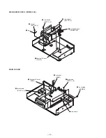
Страница 8: ... 3 lug 2 screw BVTP3 8 4 two screws BVTP3 8 4 two screws BVTP3 8 5 mechanism deck CDM36 14E 1 flat wire 23 core CN301 1 flat wire 23 core CN301 4two screws BVTP 3 8 5 main board 3 four screws BV RING 2 connector CN951 4 two screws BVTP 3 8 ...

Страница 9: ...n is pressed the following will be displayed Partial lighting 1 Partial lighting 3 Partial lighting 2 Partial lighting 1 FILTER STD 1 2 3 is displayed on the FL tube when the FILTER switch is pressed Remote commander check REMOCON PLAY is displayed on the FL tube when the PLAY button on the remote commander is pressed All go off when the other buttons a pressed Audio check Initial setting of digit...

Страница 10: ...ON OPERATIONS IN ADJ MODE The jitter value display mode can be set after the all music remaining number mode using the TIME TEXT button The functions of the number buttons are shown in the following table FUNCTIONS OF NUMBER BUTTONS With the attached remote commander MAIN BOARD Conductor Side Button Function 1 Focus bias up 2 Focus bias aliasing upper middle lower display 3 Focus bias best point j...

Страница 11: ... MUSIC SCAN ªOPEN CLOSEº and p simultaneously and the set goes in the AGING mode 3 Performing the aging for a while confirm that ERROR is not displayed on the fluorescent display tube 2 How to Exit from AGING Mode Turn off the Power and normal operation becomes ready 3 Operation sequence in AGING Mode Fig 1 In case of a failure A faulty operation mode No such as ERROR 3 is blinking During aging th...

Страница 12: ...r 3 Put disc YEDS 18 in to play the number five track 4 Confirm that oscilloscope waveform is clear and check RF sig nal level is correct or not Note A clear RF signal waveform means that the shape can be clearly distinguished at the center of the waveform RF signal waveform E F Balance 1 Track Jump Check Without remote commander Connection Procedure 1 Connect oscilloscpe to test point TP4 TE on B...

Страница 13: ... DC voltage B Traverse waveform level 1 3 0 6 Vp p Adjustment Location BD BOARD Side A MAIN BOARD Conductor Side 0 V C DC voltage Traverse waveform Tracking servo Sledding servo ON Tracking servo Sledding servo OFF RF PLL Free run Frequency Check Procedure 1 Connect frequency counter to test point MNT1 with lead wire 2 Turn ON the power 3 Put the disc YEDS 18 in to play the number five track Confi...

Страница 14: ...t for the CONTROL A1 H active 20 BUSIN I Sircs remote control signal input for the CONTROL A1 L active 21 SENSOR SW I Stabilizer detect sensor switch input terminal H active Not used open 22 CLK O Serial data transfer clock signal output to the CXD2585Q IC101 in BD section L active 23 LDON O Laser on off control signal output to the CXA2568M IC103 H laser on 24 DATA O Serial data output to the CXD...

Страница 15: ...utput terminal Not used open 43 TEX I Sub system clock input terminal Not used fixed at L 44 VDD 5V Power supply terminal 5V 45 VFDP 30V Power supply terminal 30V for FL drive 46 XSEL O Not used open 47 REINIT O Not used open 48 RFGF O Laser power hold control signal output to the CXA2568M IC103 H hold on 49 to 66 OPEN O Not used open 67 to 87 S21 to S1 O Segment drive signal output to the fluores...

Страница 16: ...rances Waveforms are taken with a oscilloscope Voltage variations may be noted due to normal produc tion tolerances Circled numbers refer to waveforms Signal path J CD c digital out Note The components identified by mark or dotted line with mark are critical for safety Replace only with part number specified Note on Printed Wiring Boards X parts extracted from the component side Through hole b Pat...

Страница 17: ... 17 Circuit Boards Location TRANS board AC SW board HP board VC SELECT board KEY board SPINDLE board DISP board MAIN board SLED board LOADING board BD board ...

Страница 18: ...Y MODE 100 mV DIV 500 ns DIV 4 IC101 LRCK 2 V DIV 10 µs DIV 6 IC101 0 WFCK 2 V DIV 100 µs DIV MAIN Board 1 IC301 XOUT 2 V DIV 20 ns DIV 1 2 0 2 Vp p Approx 570 mVp p Approx 240 mVp p 5 8 Vp p 22 8 µs 5 8 Vp p 472 µs 5 8 Vp p 136 µs 3 4 Vp p 45 MHz DISP Board 1 IC801 ª EXTAL 2 V DIV 50 ns DIV 4 2 Vp p 8 MHz 7 IC101 XPCK 2 V DIV 100 ns DIV 6 6 Vp p 230 ns ...

Страница 19: ...B820 19 20 6 3 PRINTED WIRING BOARD BD Section See page 17 for Circuit Boards Location Semiconductor Location Ref No Location D101 E 4 IC101 D 3 IC102 C 4 IC103 B 3 Q101 A 3 Q102 A 3 Page 23 Page 23 Page 25 ...

Страница 20: ...CDP XB820 6 4 SCHEMATIC DIAGRAM BD Section See page 18 for Waveforms See page 39 and 40 for IC Block Diagrams 21 22 Page 27 Page 24 Page 24 ...

Страница 21: ...ction See page 17 for Circuit Boards Location 6 6 SCHEMATIC DIAGRAM OPTICAL PICK UP MOTOR Section The components identified by mark or dotted line with mark are critical for safety Replace only with part number specified Page 23 Page 23 Page 20 Page 20 Page 22 Page 22 ...

Страница 22: ...3 D 5 D304 D 6 D305 E 6 D381 E 8 D909 B 3 D910 C 7 D911 D 3 D912 C 3 IC301 B 4 IC302 C 1 IC303 D 6 IC371 D 8 IC391 D 8 IC401 A 6 IC501 B 6 IC901 D 4 IC902 D 4 IC903 D 4 IC904 D 3 IC905 C 3 IC930 A 1 Q301 D 5 Q381 E 8 Q401 A 8 Q402 A 8 Q404 D 5 Q405 D 7 Q501 B 8 Q502 B 8 Q504 E 5 Q505 D 6 Q901 C 4 Q902 E 3 Ref No Location Page 36 Page 20 Page 26 Page 31 Page 26 ...

Страница 23: ...CDP XB820 27 28 6 8 SCHEMATIC DIAGRAM MAIN Section 1 2 See page 18 for Waveform See page 41 for IC Block Diagrams Page 21 Page 38 Page 29 ...

Страница 24: ...CDP XB820 29 30 6 9 SCHEMATIC DIAGRAM MAIN Section 2 2 Page 28 Page 33 ...

Страница 25: ...CDP XB820 31 32 6 10 PRINTED WIRING BOARDS POWER Section See page 17 for Circuit Boards Location Page 25 Page 32 Page 31 ...

Страница 26: ...CDP XB820 33 34 6 11 SCHEMATIC DIAGRAM POWER Section The components identified by mark or dotted line with mark are critical for safety Replace only with part number specified Page 30 ...

Страница 27: ...CDP XB820 35 36 6 12 PRINTED WIRING BOARDS PANEL Section See page 17 for Circuit Boards Location Page 36 Page 25 Page 35 ...

Страница 28: ...CDP XB820 37 38 6 13 SCHEMATIC DIAGRAM PANEL Section See page 18 for Waveform Page 27 ...

Страница 29: ...ital CLV MIRR DFCT FOK SERVO Interface CPU Interface OPAmp Analog SW A D Converter PWM GENERATOR FOCUS SERVO SERVO DSP SLED SERVO TRACKING SERVO TRACKING PWM GENERATOR SLED PWM GENERATOR FORCUS PWM GENERATOR 45 SIGNAL PROCESSOR BLOCK SERVO BLOCK MUTE XRST DVDD0 DATA XLAT CLOCK SENS SCLK ATSK WFCK XUGF XPCK GFS SCOR WDCK C4M DVSS0 COUT MIRR V2PO DFCT FOK PWMI LOCK MDP SSTP FETO DVDD1 SFDR SRDR TFDR...

Страница 30: ...RROR AMP TRACKING ERROR AMP VC BUFFER VCC 50µA VEE VEE VC VC VC VC VC VC VC VC VC VC VCC VEE VCC VEE VEE VC VCC LC PD LD ON HOLD SW AGC CONT RFTC RF I RF O RFE TE FE RF BOT HOLD AGC VTH LD PD A B C D VEE F E VC 1 2 3 4 5 6 7 8 9 10 11 12 13 14 15 16 17 18 19 20 21 22 23 24 VCC ...

Страница 31: ...IN XVSS AVDDR2 AVSSR2 AVDDR1 64FSO DVSS2 LVCKO CKVdd 256FSO DVDD2 R1 R1 R2 R2 AVSSR2 INVO BCKI DATA1 LRCKI INIT ATT SHIFT LATCH SYSM NU NU NU DVSS1 DVDD1 XVDD AVDDL2 L2 L2 AVSSL2 AVSSL1 L1 L1 AVDDL1 SYNC VSUB CKCTL MUTE XVDD S P ATT MODE ATT REGISTER D F TIMNG CIRCUIT 0 DETECT MUTE CIRCUIT 1024Fs CLOCK BUFFER Buffer Buffer Buffer Buffer PLM R2 PLM R1 Buffer Buffer Buffer Buffer PLM L1 PML L2 CLOCK...

Страница 32: ... 12 13 14 29 28 12 27 11 28 27 10 9 15 10 10 19 10 21 1 2 25 22 23 20 10 16 17 18 8 10 supplied with J601 not supplied 1 3 4 6 5 24 7 26 1 3 703 685 21 SCREW BV 3X8 2 4 996 687 51 KNOB AMS 3 X 4949 457 1 PANEL ASSY LOADING 4 4 950 189 01 KNOB A VOL 5 4 942 568 41 EMBLEM NO 5 SONY 6 4 997 199 21 PANEL FRONT 7 4 997 200 01 BASE L PANEL 8 4 998 790 01 KNOB POWER U 9 1 668 768 11 AC SW BOARD 10 4 951 ...

Страница 33: ... 57 A 4699 983 A MAIN BOARD COMPLETE 58 1 500 386 11 FILTER CLAMP FERRITE CORE 59 4 966 267 11 BUSHING FBS001 CORD 60 4 997 214 21 PANEL BACK 61 3 704 515 21 SCREW BV RING 62 1 575 651 21 CORD POWER T901 1 431 715 11 TRANSFORMER POWER 1 4 55 56 61 59 57 58 62 60 61 61 52 51 52 51 2 2 1 1 1 4 1 not supplied not supplied not supplied not supplied 54 54 53 T901 CDM36 14E 1 The components identified b...

Страница 34: ...ark Ref No Part No Description Remark 3 MECHANISM DECK SECTION CDM36 14E 109 4 977 896 01 PULLEY 110 4 968 905 01 BELT CDM 111 1 658 710 11 LOADING BOARD 112 4 977 891 01 PLATE GROUND 113 4 977 898 01 LEVER SWING 114 4 977 892 01 BEARING M903 A 4660 968 A MOTOR ASSY LOADING 102 1 101 108 103 1 1 BU 14E 106 106 106 104 not supplied 105 112 109 113 107 111 110 114 1 1 1 not supplied not supplied not...

Страница 35: ...S 213B F RP 161 1 775 991 11 WIRE FLAT TYPE 16 CORE 152 153 154 151 157 169 164 159 156 158 169 155 160 163 168 167 167 166 165 163 162 161 4 M901 M902 not supplied not supplied not supplied not supplied The components identified by mark or dotted line with mark are critical for safety Replace only with part number specified 162 4 993 919 01 SPRING A OP LEAF 163 4 951 940 01 INSULATOR BU 164 4 977...

Страница 36: ...AMIC CHIP 0 1uF 25V C116 1 126 209 11 ELECT CHIP 100uF 20 4V C117 1 126 209 11 ELECT CHIP 100uF 20 4V C118 1 163 275 11 CERAMIC CHIP 0 001uF 5 50V C119 1 163 231 11 CERAMIC CHIP 15PF 5 50V C120 1 163 251 11 CERAMIC CHIP 100PF 5 50V C121 1 163 021 00 CERAMIC CHIP 0 01uF 10 50V C122 1 109 982 11 CERAMIC CHIP 1uF 10 10V C123 1 163 021 00 CERAMIC CHIP 0 01uF 10 50V C124 1 164 005 11 CERAMIC CHIP 0 47u...

Страница 37: ...16 073 00 METAL CHIP 10K 5 1 10W R157 1 216 105 00 RES CHIP 220K 5 1 10W R158 1 216 105 00 RES CHIP 220K 5 1 10W R159 1 216 101 00 METAL CHIP 150K 5 1 10W R160 1 216 097 00 RES CHIP 100K 5 1 10W R161 1 216 308 00 METAL CHIP 4 7 5 1 10W R162 1 216 113 00 METAL CHIP 470K 5 1 10W R163 1 216 105 00 RES CHIP 220K 5 1 10W R168 1 216 121 00 RES CHIP 1M 5 1 10W R171 1 216 073 00 METAL CHIP 10K 5 1 10W R17...

Страница 38: ...851 1 554 303 21 SWITCH TACTILE LANGUAGE S852 1 554 303 21 SWITCH TACTILE MUSIC SCAN S853 1 554 303 21 SWITCH TACTILE AUTO SPACE S854 1 554 303 21 SWITCH TACTILE PEAK SEARCH S855 1 554 303 21 SWITCH TACTILE PLAE MODE S856 1 554 303 21 SWITCH TACTILE REPEAT S857 1 554 303 21 SWITCH TACTILE FADER S858 1 554 303 21 SWITCH TACTILE TIME TEXT 1 658 710 11 LOADING BOARD A 4699 983 A MAIN BOARD COMPLETE 3...

Страница 39: ...3T 77 D381 8 719 991 33 DIODE 1SS133T 77 D909 8 719 115 38 DIODE RD5 1JS T1B2 D910 8 719 210 21 DIODE 11EQS04 D911 8 719 991 33 DIODE 1SS133T 77 D912 8 719 991 33 DIODE 1SS133T 77 GROUND TERMINAL EB601 1 537 770 21 TERMINAL BOARD GROUND EB602 1 537 770 21 TERMINAL BOARD GROUND IC IC301 8 759 527 07 IC CXD8735N IC302 8 759 822 09 IC LB1641 IC303 8 759 710 59 IC NJM4580D D IC371 8 759 242 70 IC TC7W...

Страница 40: ... 1 6W R511 1 259 488 11 CARBON 330K 5 1 6W R512 1 259 422 11 CARBON 560 5 1 6W R513 1 259 404 11 CARBON 100 5 1 6W R517 1 249 421 11 CARBON 2 2K 5 1 4W R518 1 249 441 11 CARBON 100K 5 1 4W R519 1 249 421 11 CARBON 2 2K 5 1 4W R520 1 259 423 81 CARBON 620 5 1 6W R521 1 249 421 11 CARBON 2 2K 5 1 4W R551 1 249 435 11 CARBON 33K 5 1 4W R552 1 249 435 11 CARBON 33K 5 1 4W R553 1 249 429 11 CARBON 10K ...

Страница 41: ...NSFORMER T901 1 431 715 11 TRANSFORMER POWER 1 668 769 11 VC SELECT BOARD RESISTOR R861 1 249 415 11 CARBON 680 5 1 4W R862 1 249 417 11 CARBON 1K 5 1 4W R863 1 249 419 11 CARBON 1 5K 5 1 4W SWITCH S860 1 771 312 11 SWITCH ROTARY FILTER MISCELLANEOUS 20 1 773 216 11 WIRE FLAT TYPE 25 CORE 56 1 783 699 11 WIRE FLAT TYPE 23 CORE 58 1 500 386 11 FILTER CLAMP FERRITE CORE 62 1 575 651 21 CORD POWER 10...

Страница 42: ... 52 CDP XB820 Sony Corporation Home A V Products Company 9 922 850 11 98F057541 1 Printed in Hungary 1998 6 Published by Quality Assurance Dept Shibaura ...

Отзывы: