User Manual - twentynine
4
General Camera Architecture
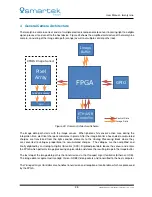
The twentynine camera series consist of multiple electronic components to convert incoming light to a digital
signal, process it and send it to the host device. Figure 24 shows the simplified architecture of the twentynine
camera, consisting of the image data path (orange) as well as multiple control paths (red).
FPGA
GPIO
Image
Buffer
ETH/USB
Controller
Control Data
Image Data
CMOS Image Sensor
Pixel
Array
Analog Processing
ADC
Figure 24: Camera Architecture Scheme
The image data path starts with the image sensor. When photons hit sensor’s active area during the
integration time, electrical charge accumulates in pixels. After the integration time has ended, accumulated
charges are transferred from the light sensitive elements to the
Analog Processing
block where they
are converted to voltages proportional to accumulated charges. The voltages are then amplified and
finally digitized by an
Analog to Digital Converter
(ADC). Digitized pixel data leaves the sensor and enters
the FPGA which performs image processing on pixel data and stores the resulting image in the image buffer.
The last step of the image data path is the transmission via the
Transport Layer Controller
(Ethernet / USB).
The image data is segmented into GigE Vision / USB3 Vision packets and transmitted to the host computer.
The
Transport Layer Controller
also handles transmission and reception of control data which are processed
by the FPGA.
35
SMARTEK Vision | User Manual - twentynine | Doc. v1.0.2


