background image


SiT9514x GUI-UM Rev 1.04


Page 23 of 95 

www.sitime.com 


GUI User Manual  

Clock Generators, Jitter Cleaners, and Network Synchronizers 


6.2.5


Bird’s Eye section


The 

Bird’s Eye

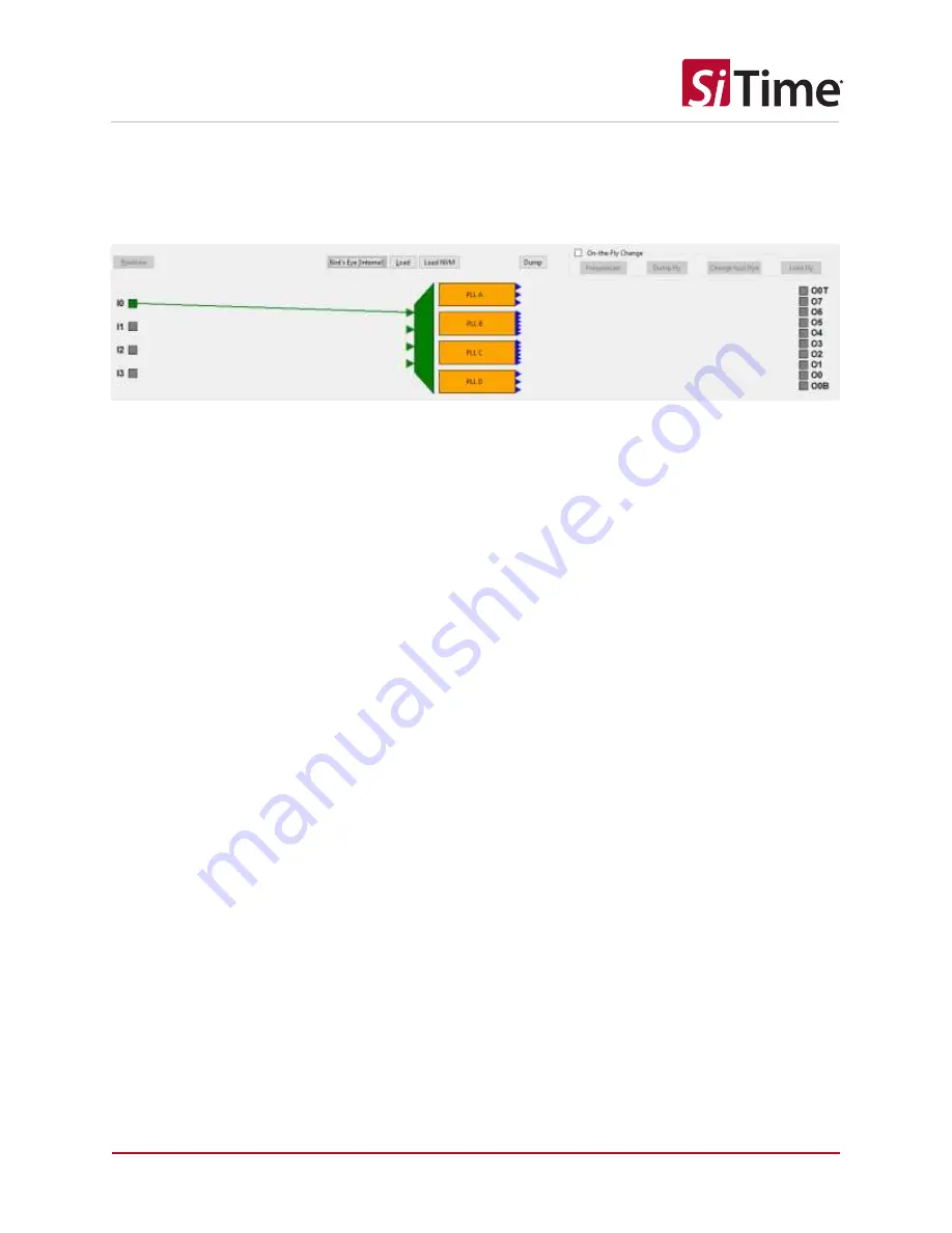
 section can be used to visualize the resulting configuration of Inputs to PLLs to Outputs. 


Figure 25: GUI Bird

s Eye section 

Click the 

Bird’s Eye

 button to activate 

the Bird’s Eye 

section, showing the configured signal paths. Click 

the 

Bird’s Eye

 button again to open the 

Bird’s Eye section in a separate window. Close that view to 

completely close the Bird’s Eye view.


This lower section of the Cascade SiTime GUI is also used to: 


Dump (save) and Load (open) device configuration files 


Specify On-the-Fly frequencies 


Change fout parameters 


Dump and Load On-the-Fly configuration parameters 


Select Realtime status of the device 

The 

Realtime

 button opens the Realtime window that displays the detailed operational status of the 

programmed device based on the current configuration. It can be is used to monitor device operation 
and view the impact of the set configuration parameters. For an example, see 

TASK 4: Use Realtime to 

set output frequency with DCO or view clock monitor status

. 

Содержание ClockSoC SiT9514 Series

Страница 1: ...6 2 1 Input Clock Reference section 19 6 2 2 Input section 20 6 2 3 PLL section 21 6 2 4 Output section 22 6 2 5 Bird s Eye section 23 7 SiT9514x device configuration tasks 24 TASK 1 Select inputs 24 SiT95141 SiT95145 input configuration 26 7 2 1 SiT95147 SiT95148 input configuration 27 7 2 2 SiT95148 clock loss configuration 28 TASK 2 Set up PLL parameters 29 TASK 3 Save or load UI configuration ...

Страница 2: ... dynamic header files 59 Using the load fly function 63 FlexIO 64 Phase sync feature 67 Input to output delay control feature 69 SiT9514x jitter attenuator as timing source for JESD204B RF converters in 5G RRU 71 7 10 1 JESD204B overview 71 Cascade as clock source for JESD204B timing signals 72 Configuring the SiT9514x for JESD204B timing signals 74 Generating SYSREF via SYSREF_REQ 74 8 Snapshots ...

Страница 3: ...lexibility in terms of frequency planning options These clocks are fully programmable with the I2C SPI interface for selecting the input frequency to output frequency translations and associated jitter attenuation loop bandwidths Using advanced design technology SiT9514x devices provide excellent jitter performance while working reliably under ambient temperatures from 40 C to 85 C These features ...

Страница 4: ...evaluation board SiT95141 10 Clock Generator Yes SiT6503EB SiT95143 10 Clock Generator No contact SiTime Technical Support to configure SiT6503EB SiT95145 10 Jitter Cleaner Yes SiT6503EB SiT95147 8 Network Synchronizer Yes SiT6502EB SiT95148 11 Network Synchronizer Yes SiT6503EB NOTE About operating parameters For this document the application was tested using Microsoft WindowsTM 10 Pro version 19...

Страница 5: ...Cleaners and Network Synchronizers 3 Cascade GUI installation Open the setup_Cascade vn n n SiTime exe file and select the folder in which to install the Cascade GUI application see Figure 1 and Figure 2 Figure 1 Selection of the destination location Figure 2 Selection of the Start Menu folder ...

Страница 6: ...Cleaners and Network Synchronizers Optionally click the checkbox to create a desktop shortcut Click Next to proceed with the installation see Figure 3 Figure 3 Option to create a desktop shortcut and proceed All SiT9514x related software is installed first see Figure 4 Figure 4 Ready to install ...

Страница 7: ...zers The SiTime evaluation boards use an FTDI chip solution for the USB to serial interface conversion The FTDI driver is installed next see Figure 5 and Figure 6 Figure 5 Installation progress Figure 6 Extracting FTDI CDM drivers Click Extract to proceed with the FTDI driver installation see Figure 7 Figure 8 and Figure 9 ...

Страница 8: ...1 04 Page 8 of 95 www sitime com GUI User Manual Clock Generators Jitter Cleaners and Network Synchronizers Figure 7 Click Next to start the device driver installation wizard Figure 8 Read and accept the license agreement ...

Страница 9: ... of 95 www sitime com GUI User Manual Clock Generators Jitter Cleaners and Network Synchronizers Figure 9 Finish the driver installation Click Finish to complete setup installation Figure 10 Figure 10 Finish the Cascade setup wizard ...

Страница 10: ... variants Select the SiT9514x variant you are using and click Select It is possible to start and use multiple instances of the application simultaneously NOTE Contact SiTime Technical Support to configure the SiT95143 device An example selection of the SiT95141 product variant is shown in Figure 11 Figure 11 Option for SiT95141 The GUI software will launch for the selected SiT95141 device variant ...

Страница 11: ... mapped to the 10 outputs offering flexible frequency translation configurations see Figure 13 The SiT95145 is a jitter attenuating frequency translation device that offers four fractional translations from the same input The four clock inputs map to all four PLLs The PLL outputs can be mapped to a subset of the 10 outputs offering flexible frequency translation configuration with independent cont...

Страница 12: ...ncy translation device that offers four independent PLLs The four clock inputs can map to any of the four PLLs The PLL outputs are mapped to the eight outputs offering flexible frequency translation configurations with independent control of each PLL in terms of jitter attenuation bandwidth control and input clock selection with redundancy see Figure 14 Figure 14 SiT95147 overall architecture ...

Страница 13: ...ting frequency translation device that offers four independent fractional PLLs PLL outputs are mapped to the 11 outputs This allows flexible frequency translation configuration with independent control of each PLL in terms of jitter attenuation bandwidth control and input clock selection with redundancy see Figure 15 Figure 15 SiT95148 overall architecture ...

Страница 14: ...ual Clock Generators Jitter Cleaners and Network Synchronizers Clock hierarchy various frequency dividers nomenclature and clock translation pathways available are shown in Figure 16 for the SiT95141 and SiT95145 devices Figure 16 SiT95141 and SiT95145 clock hierarchy ...

Страница 15: ...UI User Manual Clock Generators Jitter Cleaners and Network Synchronizers The clock hierarchy nomenclature of the various frequency dividers and clock translation pathways available for the SiT95147 are shown in Figure 17 Figure 17 SiT95147 clock hierarchy ...

Страница 16: ...GUI User Manual Clock Generators Jitter Cleaners and Network Synchronizers The clock hierarchy various frequency dividers nomenclature and clock translation pathways available on the SiT95148 device are shown in Figure 18 Figure 18 SiT95148 clock hierarchy ...

Страница 17: ...ct sets of parameters and unique to the specific sections described in detail in subsequent section of this document Chip Communication See the top left section Internal Clock Configuration See the top center section Input 0 1 2 3 See the left middle section PLL A B C D Clock Switch and Lock Loss See the center section Output 0T 7 6 5 4 3 2 1 OB See the right middle section Bird s Eye view See the...

Страница 18: ...s Chip Communication and Interrupt The Chip Communication option allows the user to specify how to connect to the chip The Interrupt section is used to configure interrupt related settings Figure 20 Communication and interrupt options Type of chip communication Either I2C or SPI can be selected Chip Connection Interrupt Related ...

Страница 19: ...ection The Input Clock Reference section is used to configure Golden clock for frequency drift monitoring Embedded MEMS frequency Figure 21 Input Clock Reference section IMPORTANT Embedded MEMS must be set to 76 86144 MHz only Operation in the 76 8 MHz setting is not generally supported and should only be used if advised to do so by SiTime Technical Support ...

Страница 20: ...ividual tabs for Input 0 3 where the following parameters can be set Frequency clock type and clock loss frequency drift FlexIO for setting Clock Switch fine and coarse frequency drift monitors for the input clocks Input assignment or not to all PLLs Figure 22 GUI Input section NOTE If no input is assigned to the PLL section then the device s internal PLL oscillator is the primary clock source ...

Страница 21: ...arameters including PLL A B C D Up to four independently configurable PLL sections Each PLL supports up to four clock inputs with Frac N dividers enabling flexible input to output frequency translation configurations PLL input clock priority settings can be changed in Page 1h registers 49h 4Bh Bandwidth Lock Loss Clock switching options SiT95145 only Input clock priorities Figure 23 GUI PLL sectio...

Страница 22: ...I Output section Additionally if the DCO mode is enabled in the Output section the Realtime section can be used to move the output frequency in the DCO mode Once the chip is programmed the Realtime section can be used for observing the status of the clock loss monitors In the Free running mode the DCO is enabled by default and is available in the Realtime section For more information see TASK 4 Us...

Страница 23: ... window Close that view to completely close the Bird s Eye view This lower section of the Cascade SiTime GUI is also used to Dump save and Load open device configuration files Specify On the Fly frequencies Change fout parameters Dump and Load On the Fly configuration parameters Select Realtime status of the device The Realtime button opens the Realtime window that displays the detailed operationa...

Страница 24: ...cy with DCO or view clock monitor status TASK 1 Select inputs The four input clocks with frequencies fin_extk translate to the PLL input clocks fink following division by the respective input dividers with fractional or integer frequency division ratios DIVN1k where the index k ϵ 0 1 2 3 Each of the PLLs are driven by one of the four divided input clocks fink as its active input clock Each PLL set...

Страница 25: ...on The DIVN1 input dividers are internally computed by the Cascade SiTime GUI software The Input section is used to set up the input frequencies and clock loss status as well as directing each input to a particular PLL Further the frequency drift monitors with respect to the inputs are set in this section An example of setting the pathways for the Input 0 clock is shown in Figure 28 ...

Страница 26: ...41 SiT95145 input configuration When an input is selected it is assigned by default to all the PLLs as input It is added to the input order of the PLLs For example if Input 0 is selected then Input 0 goes to all the PLLs as input which is also shown in the Bird s Eye section see Figure 28 Figure 28 SiT95141 Input 0 assigned to all PLLs ...

Страница 27: ...signed to a particular PLL A B C D as input and is added to the Input Order of that PLL To select an input click the tab for the selected Input 0 1 2 3 and then check the box For example if the box for Input 0 is checked it becomes the selected input for PLL A as shown in the Bird s Eye view see Figure 29 Figure 29 SiT95147 Assigning Input 0 to PLL A as input Input 0 is selected Selected Input add...

Страница 28: ...f four different clock loss conditions can be selected to initiate clock switchover for the PLL as shown in Figure 30 The PLL uses the selected information from the clock loss monitors to determine whether to enter holdover or switch to another input Figure 30 SiT95148 clock loss configuration Select the type of clock loss to be used by the chip to switch to the spare clock ...

Страница 29: ...tion by dragging the clock selections up or down in the Input Order box in the lower left area of the PLL section The priority of the input clocks is listed in order with the highest priority clock at the top of the list and the lowest priority clock at the bottom For SiT95145 only the input clock switching can be set to either Manual or Auto in the Selection drop down menu in the IP Clock Selecti...

Страница 30: ...Example of the holdover history plot Important note about the PLL bandwidth The PLL bandwidth for both fast lock and normal bandwidth is normally recommended to be less than 1 100th and 1 500th of the PLL input frequency respectively Since the PLL input frequency is determined by the Cascade SiTime GUI based on the setting for the input dividers DIVN1 the PLL bandwidth should be configured based o...

Страница 31: ...ration file Press the Send 2 Chip button top right to save the UI configuration file The GUI will prompt you to save the UI configuration file in py format to a user specified directory see Figure 33 With the Load button this file can be used to load the saved configuration later as necessary This is the preferred method to save the configuration profile Figure 33 Saving the UI configuration profi...

Страница 32: ... of 95 www sitime com GUI User Manual Clock Generators Jitter Cleaners and Network Synchronizers Figure 29 shows an example of a Cascade SiTime GUI configuration profile file Figure 34 Example content of the configuration profile file ...

Страница 33: ...al Clock Generators Jitter Cleaners and Network Synchronizers Click the Send 2 Chip button top right to program the chip with the current configuration or a previously loaded configuration profile see Figure 35 Figure 35 Example of successful programming of a SiT95147 ...

Страница 34: ...PI is selected then the NVM SPI write file is created To dump the NVM or I2C SPI writes file the file must first be activated using the Send 2 Chip button even if the SiTime evaluation board is not connected This runs the algorithms that optimize the internal configuration based on the required inputs and outputs After this the Dump button can be used to save the list of register writes see Figure...

Страница 35: ...n the Dump button is clicked the user is prompted to save the configuration to a file Select the NVM I2C SPI write option from the drop down Use the Legacy State NVM NVM option in this case which allows the user to save the file to any directory location needed see Figure 37 Figure 37 Saving the NVM Saves the NVM I2C SPI write file ...

Страница 36: ...nchronizers Figure 38 shows an example of an NVM I2C write file Figure 38 Example NVM I2C write file Figure 39 shows an example of an NVM SPI write Figure 39 Example NVM SPI write file The NVM file can be directly written to the chip using the Load NVM button but it cannot be used to load the UI configuration profile ...

Страница 37: ...ork Synchronizers 7 4 3 Saving efuse NVM py I2C SPI files Select the NVM I2C SPI write option from the drop down Use the EFUSE Locking efuse NVM py option for this case This allows the user to save the file to any directory see Figure 40 Figure 40 Saving Efuse NVM I2C SPI files Saves the Efuse NVM I2C SPI write ...

Страница 38: ...anual Clock Generators Jitter Cleaners and Network Synchronizers Figure 41 shows an example of an Efuse NVM I2C write file Figure 41 Example Efuse NVM I2C write file Figure 42 shows an example of an Efuse NVM SPI write file Figure 42 Example Efuse NVM SPI write file ...

Страница 39: ...k Generators Jitter Cleaners and Network Synchronizers 7 4 4 Saving the Cascade SiTime GUI state The state of the Cascade SiTime GUI i e the values of the widgets can be saved as a json file Figure 43 Saving the state of the Cascade SiTime GUI Saves the state of GUI json file ...

Страница 40: ...ge 40 of 95 www sitime com GUI User Manual Clock Generators Jitter Cleaners and Network Synchronizers Figure 44 Loading files using the Cascade SiTime GUI Load loads the UI configuration file Load NVM loads the NVM I2C write file ...

Страница 41: ...rk Synchronizers 7 4 5 Using the load NVM function When the Load button is pressed an open file dialog window pops up Navigate to select the Cascade SiTime GUI configuration file see Figure 45 Figure 45 Using the Load function Note the state of the Cascade SiTime GUI json file can be loaded using the Load button ...

Страница 42: ...ronizers When a Cascade SiTime GUI configuration file is loaded the programmed configuration is shown in the GUI See Figure 46 for an example showing a basic SiT95141 variant configuration Examples for other SiT9514x variants are shown in the subsequent figures Figure 46 Showing the programmed configuration for SiT95141 ...

Страница 43: ...SiT9514x GUI UM Rev 1 04 Page 43 of 95 www sitime com GUI User Manual Clock Generators Jitter Cleaners and Network Synchronizers Figure 47 Showing the programmed configuration for SiT95145 ...

Страница 44: ...SiT9514x GUI UM Rev 1 04 Page 44 of 95 www sitime com GUI User Manual Clock Generators Jitter Cleaners and Network Synchronizers Figure 48 Showing the programmed configuration for SiT95147 ...

Страница 45: ...SiT9514x GUI UM Rev 1 04 Page 45 of 95 www sitime com GUI User Manual Clock Generators Jitter Cleaners and Network Synchronizers Figure 49 Showing the programmed configuration for SiT95148 ...

Страница 46: ...ors Jitter Cleaners and Network Synchronizers 7 4 6 Using the load NVM function Load NVM loads the NVM I2C sequence of writes file When the Load NVM button is clicked it prompts the user to load an NVM I2C write file see Figure 50 Figure 50 Loading the NVM I2C sequence of writes file ...

Страница 47: ...the selected configuration even with the SiTime evaluation board disconnected Figure 51 Descriptions of the Realtime section When the Return button is clicked the Realtime Window closes and focus returns to the main window The Register Manipulation sub section allows the user to read or write to a specified register on the selected page see Figure 51 Select a Page to view its Registers Type in whi...

Страница 48: ...ealtime view can be used to change the output frequency using the DCO feature or to check the status of all clock monitors see Figure 52 Figure 52 Viewing the Realtime section after the chip is programmed Set the PPM change desired here 10 ppm in this example Use the button to increase frequency and button to decrease frequency Click Continuous Read to log continuous Real Time information from Clo...

Страница 49: ...ter Cleaners and Network Synchronizers 7 5 1 Interrupts Click the INTRB EDIT button to open the Interrupt Defect Selection panel to enable or disable sticky notifications on the INTRB pin see Figure 53 Figure 53 Selecting the interrupt defects to enable sticky notifications on the INTRB pin ...

Страница 50: ...ners and Network Synchronizers Click the Clear button to clear all sticky notifications on the chip see Figure 54 and clear the INTRB pin whose state should now be 1 assuming no defect exists now among the selected list Figure 54 Using the Clear button Clcik the Clear button to clear the interrupts ...

Страница 51: ...tter Cleaners and Network Synchronizers 7 5 2 On the fly change Select the On the fly Change checkbox to enable the on the fly change feature allowing the user to enter frequencies Figure 55 Enabling on the fly change feature Select On the Fly Change to enable the on the fly change feature ...

Страница 52: ...cies Near the bottom of the panel is the New Hz field where you can enter a new frequency and then click the button right of the field to add the new frequency to the list see Figure 56 Figure 56 Using the On the Fly Frequency pop up After the chip is programmed the dump fly and load fly functions are enabled Note if the connection to the chip is not active you will not be able to operate this fea...

Страница 53: ...tput per PLL When the Dump Fly button is clicked it prompts the user to dump the NVM I2C write file see Figure 57 Note the number of files created are 4 N N number of frequencies entered The created file will have fixed file name Example PllX_pin_fout_otf_NVM py X A B C D pin Output name Example if OUT6 it will be displayed as 6 fout Frequency that are entered in the Frequency box If the frequency...

Страница 54: ...ned appropriately see Figure 58 Figure 58 Selecting static profile on the fly with multiple same frequency outputs The output files will look different from the single output files as shown below Example PllX_pin1_fout_pin2_fout_ otf_NVM py If the frequency entered was 125 MHz then the file created will be like the following example X A B C D pin1 2 output names Example if OUT6 it will be displaye...

Страница 55: ...ions The src directory has the following files dyn_change_out_fout py flymode_freq_change_latest_multi py The main function is in the file named dyn_change_out_fout py If this python file is opened in an editor at the end of the file the dyn_change_out_fout function is called with three inputs as follows 1 DIR Path to the directory where the following two files were created OntheFly_globals json O...

Страница 56: ...ate a dynamic profile that uses on the fly frequencies first create the list of the frequencies required and then save it this should be done before chip programing Then create additional files for each frequency defined in the initial list that separates files with the appropriate file names e g PllA_0T_125000000p0_otf_nvm as the file name for output 0T connected to PLLA with frequency 125 MHz ...

Страница 57: ... Description of Dynamic State Files OntheFly_globals json This file contains the variables set for dynamic changes Note the file is formatted for easy reading see Figure 60 Figure 60 OntheFly_globals json OntheFly_current_fvco_fout json This file has the current FOUTs and FVCOs which get updated when the dynamic function is run ...

Страница 58: ...aners and Network Synchronizers After Step 1 the outputs that need to be changed would have updated frequency in this example 5 out_fout 5 that comes from PLL B being changed and therefore is the frequency of PLL B pll_fvco N as set in Task 1 see Figure 61 Figure 61 OntheFly_current_fvco_fout json ...

Страница 59: ...time com GUI User Manual Clock Generators Jitter Cleaners and Network Synchronizers 7 5 6 Description of dynamic header files OntheFly_globals h Has the variables set for dynamic changes see Figure 62 Figure 62 Description of dynamic header files ...

Страница 60: ...ser Manual Clock Generators Jitter Cleaners and Network Synchronizers After dumping the static files in a folder the Change fout Dyn button will be highlighted after dumping the static files in a folder Figure 63 Using the Change fout Dyn button Change fout Dyn ...

Страница 61: ...y Dynamic Frequency After the OK button is pressed the output file will be created in the exe directory Example fout_pin1_freq_pin2_freq_ otf_NVM py If the frequency selected was 156250000 5 then the file created will be like the following fout__5_156250000 0 py pin1 2 output names Example if OUT0B it will displayed as 0B fout frequency that is selected in the Frequency change dropdown Select the ...

Страница 62: ...Rev 1 04 Page 62 of 95 www sitime com GUI User Manual Clock Generators Jitter Cleaners and Network Synchronizers The python output file would look like that in Figure 65 Figure 65 On the fly python output file example ...

Страница 63: ...fly function When the Load Fly button is clicked it prompts the user to load the NVM I2C write file created by the on the fly change feature see Figure 66 Figure 66 Using the Load Fly button Load Fly Loads the NVM I2C write files Load NVM I2C write files created for On the Fly Change Load py extension files created for On the Fly Change feature ...

Страница 64: ...clocks Notify of the PLL defects The Edit button in the FlexIO section will open a pop up to select these options Five possible outputs can be assigned to any FlexION output shown in Figure 67 as follows Clock Monitoring Defect Clock Notify PLL Notify All Notify both Clock Notify and PLL Notify INTRB INTRB Figure 67 Using the GUI FlexIO widget for SiT95147 A summary of the selections made is avail...

Страница 65: ...zers The FlexIO Settings panels for SiT9514x differ depending on the chip type Figure 68 shows the FlexIO Settings panels for SiT95141 SiT95145 SiT95147 panel A and SiT95148 panel B Figure 68 FlexIO settings differentiation depending on the device series type A FlexIO section for SiT95141 SiT95145 SiT95147 B for SiT95148 A B ...

Страница 66: ...ect FlexIO 3 for PLL A lock loss signal monitoring the summary of the selections made is available in the Flex IO section see Figure 69 Figure 69 Example using the FlexIO settings for SiT95148 FlexIO 3 selected PLL A loss of lock notification selected A summary of the selections made is available in the Flex IO section once the Flex IO Settings window is closed ...

Страница 67: ...are used as subordinate PLLs that work on an internal XO reference that is derived from the output of PLLA Using this feature is recommended only for cases where the output phases are expected to stay in sync across PLLs even with loss of the input clock For all other cases using this is not recommended Figure 70 shows the PLL phase sync section in the GUI Once the Phase Sync check box is clicked ...

Страница 68: ...his synchronization is not possible the GUI will report the appropriate output and the internal frequency used The user may change the output frequency to allow the multiples of the LCM of output frequency and the internal frequency OCXO to be within the frequency band 6 7 GHz 8 4 GHz An example error message is shown below Figure 71 Example of 85 MHz 125 MHz fall error message In the example show...

Страница 69: ...me across multiple power ups with a total uncertainty of 175 ps o The delay parameter shown above is consistent across multiple power cycles where Delay A Fixed delay 175 ps Input 3 Sync Mode of operation The output always starts with a fixed phase relationship to the rising edge of an independent clock on Input 3 across multiple power ups of the chip see Figure 73 o The start of the output clock ...

Страница 70: ... to output delay across multiple power ups in sync mode The Input 3 IN3 SYNC is a per PLL feature and can be enabled for each PLL selectively in the GUI see Figure 74 This can be a very useful feature where the Input 3 clock can be used as an independent SYNC Figure 74 Example showing the selection Input 3 SYNC for PLLA of SiT95148 IN3 Sync Mode ...

Страница 71: ...04B is a JEDEC standard which defines a high speed serial interface link between data converters and logic devices A block diagram of a JESD204B link showing the data link and timing signals is shown in Figure 75 Clock IC High speed serial link JESD204 Receiver JESD204 Transmitter SYNC Device Clock SYSREFTX Device Clock SYSREFRX Figure 75 Block diagram of JESD204B interface between ADC Transmitter...

Страница 72: ...0 4 I N T E R F A C E IN0 IN1 IN3 For ZDB FlexIO13 SYSREF_REQ SYSREF Request SYNC SYNC SYSREF_REQ Device Clock SYSREF SYNC M DACs Figure 76 eCPRI clocked 5G RRU clock tree designed around SiT95148 and JESD204 compliant RF FE In the above 5G RRU application SiT9514x synthesizes multiple copies of the device clock DEV_CLK and a divided down phase locked SYSREF from one of the two master clock refere...

Страница 73: ...In this configuration SYSREF_REQ trigger serves as a gating signal for the PLLB output divider DIVO5 PLLB is configured to generate SYSREF as a divided down phase locked copy of Dev_CLK The SYSREF_REQ is used as a gating signal to the internally generated SYSREF clock SYREF is gated into the output driver when SYSREF_REQ is high and gated off when SYSREF_REQ is low thereby driving OUT5 to a logica...

Страница 74: ...lay buffer ZDB mode Feed the output of the SYSREF fan out buffer into Input 3 configured for ZDB mode This will ensure a repeatable and zero phase delay between the DEV_CLK and SYSREF pairs The following sections describe the procedure to configure SYSREF generation using two types of stimulus hardware trigger signal SYSREF_REQ on FLEXIO13 or by writing once each to multiple registers Generating S...

Страница 75: ...rators Jitter Cleaners and Network Synchronizers 2 Go to Page 0 reg 0xFF 0x00 or go to the Generic page in the Realtime Window see Figure 79 Figure 79 Selecting the Generic page in the Realtime Window s Register Manipulation section of SiT95148 for JESD204B Select the Generic page ...

Страница 76: ...wn in Table 2 as set in the previous example where PLLB register 0x19 00100010b 0x22 see Figure 80 Figure 80 Writing the value to Register 0x19 in the Realtime section of SiT95148 for JESD204B 4 Do a small trigger update An example I2C script is shown below i2c i2cw 0x69 0x0f 0x00 i2c i2cw 0x69 0x0f 0x04 i2c i2cw 0x69 0x0f 0x00 Write button Value Generic page Reg 0x19 ...

Страница 77: ...nual Clock Generators Jitter Cleaners and Network Synchronizers 5 Go to PLL page 0xFF 0x0B For the parameters shown in the example above for PLLB see Figure 81 Figure 81 Selection of the PLL B page in the Realtime section of SiT95148 for JESD204B PLL B page selected ...

Страница 78: ...tive encoding see Figure 82 of the SYSREF output This means that SYSREF can be connected to the one of the PLL outputs and to decode it in register 0x09 we need to write appropriate value for PLL B For example if PLLB Output 5 is the SYSREF output write 0x08 001000b to register 0x09 see Figure 82 Figure 82 SiT95148 overall clock hierarchy E g PLLB OUT5 is SYSREF output 0 0 1 0 0 0 ...

Страница 79: ...ep this bit low 0 5 Keep this bit high 1 6 7 Do not change the values default is 0 0 Generating SYSREF via registers SYSREF generation can also be controlled by toggling bit 1 of register 0x05 in the respective PLL The following steps outline the procedure to gate SYSREF on a specific output using register writes 1 Follow steps 1 to 6 as described in the previous section 2 Register 0x05 bit 1 1 is...

Страница 80: ...t set bit 1 high see Figure 84 Figure 84 Write bit 1 high to the Page PLL B Register 0x05 of the SiT95148 to enable SYSREF b Disable SYREF on the selected output set bit 1 low see Figure 85 Figure 85 Write bit 1 low to the Page PLL B Register 0x05 of the SiT95148 to disable SYREF Write button Value PLL B Page Register 0x05 Write button Value PLL B Page Register 0x05 ...

Страница 81: ...SiT9514x GUI UM Rev 1 04 Page 81 of 95 www sitime com GUI User Manual Clock Generators Jitter Cleaners and Network Synchronizers 8 Snapshots of specific use case scenarios Figure 86 Free run scenario 1 ...

Страница 82: ...SiT9514x GUI UM Rev 1 04 Page 82 of 95 www sitime com GUI User Manual Clock Generators Jitter Cleaners and Network Synchronizers Figure 87 Free run scenario 2 ...

Страница 83: ...SiT9514x GUI UM Rev 1 04 Page 83 of 95 www sitime com GUI User Manual Clock Generators Jitter Cleaners and Network Synchronizers Figure 88 Lock scenario 1 ...

Страница 84: ...SiT9514x GUI UM Rev 1 04 Page 84 of 95 www sitime com GUI User Manual Clock Generators Jitter Cleaners and Network Synchronizers Figure 89 Lock scenario 2 ...

Страница 85: ...ime com GUI User Manual Clock Generators Jitter Cleaners and Network Synchronizers Free running DCO After programming the chip click the Realtime button to use the DCO mode see Figure 90 Figure 90 Free Running DCO Mode configuration Realtime button ...

Страница 86: ...SiT9514x GUI UM Rev 1 04 Page 86 of 95 www sitime com GUI User Manual Clock Generators Jitter Cleaners and Network Synchronizers Figure 91 Hitless Switch Phase Build Out setting Select Phase Build Out ...

Страница 87: ...v 1 04 Page 87 of 95 www sitime com GUI User Manual Clock Generators Jitter Cleaners and Network Synchronizers Figure 92 Clock Switch Phase Propagation and Slope settings Select Phase Propagation and Phase Slope settings ...

Страница 88: ...e internal feedback dividers and cancelling the delays introduced by the internal dividers and clock distribution pathways The Input 3 pins are used as the external feedback and any of the outputs from the PLL which is being set up in ZDB mode should be routed to the Input 3 differential inputs SiTime recommends using Input 0 as the input clock when using Input 3 as the external feedback clock in ...

Страница 89: ...rs Jitter Cleaners and Network Synchronizers 9 Low wander mode Low wander mode provides the best jitter cleaning by employing a dual loop PLL see Figure 94 Refer to the datasheet and application note for a complete description Figure 94 Selecting low wander mode Select Low Wander Mode ...

Страница 90: ...n Output placement and frequency planning The output placement and frequency planning should be such that outputs with a frequency difference in the range 12 kHz to 20 MHz should not be placed next to each other and should be spaced as far apart as possible to minimize output to output coupling leading to in band spurs Figure 95 Example where outputs O3 and O2 should be spaced apart ...

Страница 91: ...SiT9514x GUI UM Rev 1 04 Page 91 of 95 www sitime com GUI User Manual Clock Generators Jitter Cleaners and Network Synchronizers Figure 96 Optimal profile outputs re arranged to minimize spurs ...

Страница 92: ...OS outputs avoid up to the third harmonic of the adjacent LVCMOS output to land within the integration frequency band of the jitter sensitive output frequency see Figure 97 For Outputs O5 O3 156 25 MHz a crosstalk spur location may occur due to adjacent placement of the 50 MHz LVCMOS 50 MHz outputs 156 25 MHz 3 50 MHz 6 25 MHz Figure 97 Third harmonic of the adjacent LVCMOS output ...

Страница 93: ... setting the Single Ended CMOS output format it is recommended to always select complimentary outputs to minimize single ended CMOS output to differential output coupling For complimentary CMOS format the output type Output OT selection should be with ON and OP selected ON CLKN and OP CLKP Figure 98 Example of an incorrect profile for complimentary CMOS format ...

Страница 94: ...SiT9514x GUI UM Rev 1 04 Page 94 of 95 www sitime com GUI User Manual Clock Generators Jitter Cleaners and Network Synchronizers Figure 99 Optimal profile for complimentary CMOS format ...

Страница 95: ...ms any and all express or implied warranties either in fact or by operation of law statutory or otherwise including the implied warranties of merchantability and fitness for use or a particular purpose and any implied warranty arising from course of dealing or usage of trade as well as any common law duties relating to accuracy or lack of negligence with respect to this material any SiTime product...

Отзывы: