background image

                                                                    Smart Machine Smart Decision


SIM868_Series_Hardware_Design_V1.06

                       49                                    

2017-07-13


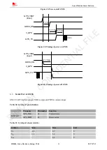
Figure 43: Power on/off GNSS 

GPS_VBAT

GNSS_EN

GPS_TX

(input)

T

1

=1s

NEMA

V_GPS

T

2

=1.6s T

2

=1.9s


Figure 44: Timing of power on GNSS 

GPS_VBAT

GNSS_EN

GPS_TX

(input)

T

1

=3.4s

NEMA

V_GPS


Figure 45: Timing of power off GNSS 


6.5.


Serial Port of GNSS 

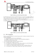
GNSS UART interface support NMEA output and PMTK command input.   

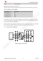
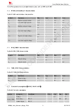
Table 30: Serial port pin definition 

Table 31: Serial port characteristics 

Symbol 

Min 

Max 

Unit 

V

IL


-0.3 

0.7 

V

IH


2.1 

3.0 

V

OL


0.4 


Pin name 

Pin number  Function 

Serial port 

GPS_TXD 

61 

Transmit data 

GPS_RXD 

62 

Receive data 

SIMCOM   

CONFIDENTIAL 

FILE

Содержание SIMCom SIM868 Series

Страница 1: ...SIM868_Series_Hardware_Design_V1 06 S I M C O M C O N F I D E N T I A L F I L E...

Страница 2: ...possession Furthermore system validation of this product designed by SIMCom within a larger electronic system remains the responsibility of the customer or the customer s system integrator All specif...

Страница 3: ...rt 26 5 3 1 Power on GSM 26 5 3 2 Power off GSM 27 5 4 Power Saving Mode of GSM 28 5 4 1 Minimum Functionality Mode of GSM Part 28 5 5 Serial Port of GSM 29 5 5 1 Function of Serial Port 30 5 5 2 Seri...

Страница 4: ...tion Modes of GNSS 52 6 10 A GPS 54 6 10 1 Easy Mode 54 6 10 2 EPO 54 6 11 Fast Fix 54 6 12 Multi tone AIC 55 6 13 SBAS 55 7 PCB Layout 56 7 1 Pin Assignment 56 7 2 Principle of PCB Layout 57 7 2 1 An...

Страница 5: ...9 Manufacturing 63 9 1 Top and Bottom View of SIM868 63 9 2 Typical Solder Reflow Profile 63 9 3 The Moisture Sensitivity Level 64 9 4 Baking Requirements 64 10 Packaging 65 11 Appendix 67 11 1 Relat...

Страница 6: ...F THE I2C 41 TABLE 21 PIN DEFINITION OF THE ADC 41 TABLE 22 ADC SPECIFICATION 42 TABLE 23 PIN DEFINITION OF THE NETLIGHT 42 TABLE 24 STATUS OF THE NETLIGHT 42 TABLE 25 PIN DEFINITION OF THE STATUS 43...

Страница 7: ...STURE SENSITIVITY LEVEL AND FLOOR LIFE 64 TABLE 47 BAKING REQUIREMENTS 64 TABLE 48 TRAY SIZE 65 TABLE 49 SMALL CARTON SIZE 66 TABLE 50 BIG CARTON SIZE 66 TABLE 51 RELATED DOCUMENTS 67 TABLE 52 TERMS A...

Страница 8: ...UIT 32 FIGURE 22 RX LEVEL MATCHING CIRCUIT 32 FIGURE 23 USB REFERENCE CIRCUIT 32 FIGURE 24 CONNECTION FOR SOFTWARE UPGRADING 33 FIGURE 25 UART1_RI BEHAVIOUR OF VOICE CALLING AS A RECEIVER 34 FIGURE 26...

Страница 9: ...PASSIVE ANTENNA MATCHING CIRCUIT 51 FIGURE 50 GNSS ACTIVE ANTENNA MATCHING CIRCUIT 52 FIGURE 51 PIN ASSIGNMENT 56 FIGURE 52 TOP AND BOTTOM VIEW OF SIM868 63 FIGURE 53 TYPICAL SOLDER REFLOW PROFILE OF...

Страница 10: ...24 1 02 1 Add Application Mode 2 Add Power Supply of GNSS 3 Add Power Saving Mode of GNSS 4 Add operation mode of GNSS 5 Modify Backup Power of GNSS 6 Add software upgrading in Simultaneous mode 7 Add...

Страница 11: ...low as 167dBm signal even without network assistance The GNSS has excellent low power consumption characteristic acquisition 24mA tracking 22mA GNSS supports various location and navigation applicati...

Страница 12: ...S GPRS data downlink transfer max 85 6 kbps GPRS data uplink transfer max 85 6 kbps Coding scheme CS 1 CS 2 CS 3 and CS 4 PAP protocols for PPP connect Integrate the TCP IP protocol Support Packet Bro...

Страница 13: ...le 3 Key Features of GNSS Part Parameter Description Performance Min Typ Max Unit Power supply Power supply 2 9 3 4 4 V Horizontal Position Accuracy 1 Autonomous 2 5 m Velocity Accuracy 2 Without Aid...

Страница 14: ...port NMEA Power consumption With GPS only mode 4 Acquisition 24 5 mA Continuous tracking 22 2 mA GLP current 12 mA Sleep current 6 5 mA Stop current 490 uA Backup current 8 uA Power consumption With B...

Страница 15: ...onsumption depends on network settings such as DTX off on FR EFR HR hopping sequences and antenna GPRS STANDBY Module is ready for GPRS data transfer but no data is currently sent or received In this...

Страница 16: ...sted or not 2 3 Functional Diagram Figure 1 shows the block diagram of SIM868 GSM baseband PMU The GSM Radio Frequency part Antenna interface GNSS interface Other interface Figure 1 SIM868 block diagr...

Страница 17: ...S USB_DM GSM_ANT STATUS SIM1_VDD MCCA3 GND UART2_RXD GND GPS_RXD GNSS_EN 1PPS GPIO2 GPS_TXD 13 SPK1N UART1_RI GPS_ANT 14 15 16 21 17 18 19 20 22 23 24 25 26 27 28 29 30 31 32 33 37 36 35 34 1 42 41 40...

Страница 18: ...P 9 I Differential audio input If these pins are unused keep open MICN 10 SPK1P 11 O Differential audio output SPK1N 12 SPK2P 44 SPK2N 43 GNSS interface GPS_RXD 62 I Receive data If these pins are unu...

Страница 19: ...SCL 65 O I2C serial bus clock SIM card interface SIM1_VDD 18 O Voltage supply for SIM card Support 1 8V or 3V SIM card All signals of SIM interface should be protected against ESD SIM1_DATA 15 I O SI...

Страница 20: ...Smart Machine Smart Decision SIM868_Series_Hardware_Design_V1 06 19 2017 07 13 3 3 Package Dimensions Figure 3 Dimensions of SIM868 Unit mm S I M C O M C O N F I D E N T I A L F I L E...

Страница 21: ...Smart Machine Smart Decision SIM868_Series_Hardware_Design_V1 06 20 2017 07 13 Figure 4 Recommended PCB footprint outline S I M C O M C O N F I D E N T I A L F I L E...

Страница 22: ...Smart Machine Smart Decision SIM868_Series_Hardware_Design_V1 06 21 2017 07 13 Figure 5 Recommended SMT stencil footprint outline S I M C O M C O N F I D E N T I A L F I L E...

Страница 23: ...ure 6 a 10K resistor should be added between GPIO1 and GNSS_EN pin In this mode GNSS part can be enabled through AT command AT CGNSPWR 1 and disabled through AT command AT CGNSPWR 0 GSM and GNSS s fir...

Страница 24: ...work independently It s convenient for customer to control them separately Figure 7 is the block diagram of this mode Module VRTC VRTC PWRKEY MCU UART1_TXD UART1_RXD RXD1 TXD1 GSM_VBAT LDO Adapter 5V...

Страница 25: ...ly recommended which can prevent chip from damaging by the voltage surge These capacitors and zener diode should be placed as close as possible to GSM_VBAT pin Table 7 Recommended zener diode Vendor P...

Страница 26: ...with the 2A peak current in burst mode of the GSM Figure 11is the reference circuit Vin Vout FB U101 1 2 3 4 5 LM2596 ADJ 100uH MBR360 L101 C101 C102 D10 2 C103 R102 R101 FB101 330uF GSM_VBAT 2 2K 1K...

Страница 27: ...shown as below 4 7K 47K Turn on off impulse PWRKEY Power on off logic 100K 3V GSM 1K Figure 13 Powered on off GSM using transistor PWRKEY Power on off logic 100K 3V GSM 1K Figure 14 Powered on off GSM...

Страница 28: ...STATUS VIL 0 7V Serial port Undifined Active input T3 2s 1 5s T1 33s T2 2s Figure 16 Timing of power off GSM Note 1 The GSM will restart after pulling down the PWRKEY over 33 seconds 2 VDD_EXT will p...

Страница 29: ...de AT command AT CSCLK 1 can be used to set GSM into sleep mode AT command AT CFUN fun can be used to set GSM into minimum functionality When GSM is in sleep mode and also in minimum functionality mod...

Страница 30: ...al port can report URC but it cannot input AT command Only after the DTR pin is pulled to low level for 50ms the serial port can input AT command 5 4 1 3 Sleep Mode 2 AT CSCLK 2 In this mode GSM will...

Страница 31: ...ore attention to the following requirements Synchronization between DTE and DCE When DCE powers on with autobauding enabled it is recommended to send AT or at or aT or At to synchronize the baud rate...

Страница 32: ...wing figure from5 6K to 14K 1K 5 6K RXD TXD RTS CTS GPIO GPIO EINT DTE 3 3V 5 6K 5 6K 1K 1K 1K 1K 1K 1K GSM UART1_TXD UART1_RXD UART1_RTS UART1_CTS UART1_DTR UART1_DCD UART1_RI GND GND Figure 19 Resis...

Страница 33: ...t 5 5 3 Debug Interface GSM could be debugged through USB port The recommended diagram is shown as Figure 23 GSM USB GND GND 22R USB_VBUS VBUS 1uF USB_DM USB_DP USB_DM 22R USB_DP Figure 23 USB referen...

Страница 34: ...GND and PWRKEY pin to IO connector for the upgrading and PWRKEY pin should be connected to GND while upgrading Refer to Figure 24 for debugging and upgrading software UART1_TXD GSM DCE UART1_RXD GND P...

Страница 35: ...ed as caller the UART1_RI will remain high Please refer to Figure 27 HIGH LOW Idle Ring Establish the call Hang up the call Idle RI Figure 27 UART1_RI behaviour as a caller 5 7 Audio Interfaces GSM pa...

Страница 36: ...adjust the input gain level of microphone AT command AT SIDET is used to set the side tone level In addition AT command AT CLVL is used to adjust the output gain level For more details please refer t...

Страница 37: ...g voltage 1 9 2 2 V Working current 2 0 mA Input impedance differential 13 20 27 K Idle channel noise 67 dBm0 SINAD Input level 40dBm0 29 dB Input level 0dBm0 69 dB Table 16 Audio output characteristi...

Страница 38: ...e GSM Phase 1 specification and the new GSM Phase 2 specification for FAST 64kbps SIM card Both 1 8V and 3 0V SIM card are supported The SIM interface is powered from an internal regulator in the modu...

Страница 39: ...7 10M 006 512 22pF VCC GND RST VPP CLK I O SIM_VDD SIM_RST SIM_CLK SIM_DATA ESDA6V1 SIM_DET 22R 22R 22pF 22R 22pF Figure 31 Reference circuit of the 6 pin SIM card holder 5 8 2 SIM Card Design Guide S...

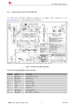
Страница 40: ...molex com for more information about the holder Figure 32 Molex 91228 SIM card holder Table 18 Pin description Molex SIM card holder Pin name Signal Description C1 SIM_VDD SIM card power supply C2 SIM...

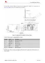
Страница 41: ...33 Amphenol C707 10M006 512 SIM card holder Table 19 Pin description Amphenol SIM card holder Pin name Signal Description C1 SIM_VDD SIM card power supply C2 SIM_RST SIM card reset C3 SIM_CLK SIM car...

Страница 42: ...n Table 20 Pin definition of the I2C Note 1 I2C should be pulled up to 2 8V via 4 7K resistor externally 2 I2C function is not supported in the standard firmware If you need please contact SIMCom 5 11...

Страница 43: ...IGHT Status SIM868 behavior Off Powered off 64ms On 800ms Off Not registered the network 64ms On 3000ms Off Registered to the network 64ms On 300ms Off GPRS communication is established Reference circ...

Страница 44: ...it burst 5 15 Antenna Interface of GSM Antenna interface of GSM The input impendence of the antenna should be 50 and the VSWR should be less than 2 It is recommended that the GSM antenna should be pla...

Страница 45: ...101 and C102 are used for antenna matching the value of the components can only be got after the antenna tuning usually they are provided by antenna vendor By default the R101 is 0 resistor and the C1...

Страница 46: ...Antenna matching circuit should be close to the antenna Keep the RF traces impedance as 50 The RF traces should be kept far away from the high frequency signals and strong interference source 5 17 Bl...

Страница 47: ...0 Modem off BT on Interval 500ms 1250ms Normal 880ms 3 BLE Connection 14 3 Modem off BLE on Connection Interval 380ms 4 BLE FMP 17 1 Modem off BLE on BLE Connected Press Find my device 5 BLE PXP 17 9...

Страница 48: ...baud rate is 9600 115200bps Determine by firmware 6 2 Power Supply of GNSS The power supply range of GNSS is from 2 9V to 4 4V Recommended voltage is 4 0V The power supply must be able to provide suf...

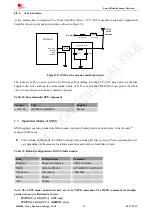
Страница 49: ...al Power Module Power Supply LDO DCDC LDO GNSS Part Backup Domain GPS_VBAT VRTC 2 3 4 3V External power Figure 42 RTC supply from external power 6 4 Power on off GNSS The GNSS is controlled by GNSS_EN...

Страница 50: ...GPS_TX input T1 3 4s NEMA V_GPS Figure 45 Timing of power off GNSS 6 5 Serial Port of GNSS GNSS UART interface support NMEA output and PMTK command input Table 30 Serial port pin definition Table 31...

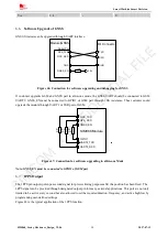
Страница 51: ...he module through UART1 or USB port of GSM GPS_TXD SIM868 Module GPS_RXD GNSS_EN UART2_TXD UART2_RXD R1 0R GPIO1 R2 0R R3 10K Figure 47 Connection for software upgrading in all in one Mode Note GNSS_E...

Страница 52: ...lement e g the ceramic patch the helix structure and chip antennas Sometimes it also contains a passive matching network to match the electrical connection to 50 impedance The most common antenna type...

Страница 53: ...ound Table 32 Recommended BPF component Package Type Supplier 1 10 0 90 SAFFB1G56KB0F0A Murata 6 9 Operation Modes of GNSS GNSS supports operating modes like full on mode stop mode backup mode periodi...

Страница 54: ...reduce power consumption PMTK225 Type Run time Sleep time Second run time Second sleep time 15 Note Using the PMTK225 command to set periodic mode Periodic backup mode PMTK225 0 2B PMTK223 1 25 180000...

Страница 55: ...t receiving the broadcast ephemeris After a while generally tens of seconds 3 day extensions will be completely generated then all Easy functions will be maintained at a standby condition Easy assista...

Страница 56: ...BAS SBAS is the abbreviation of Satellite Based Augmentation System The SBAS concept is based on the transmission of differential corrections and integrity messages for navigation satellites that are...

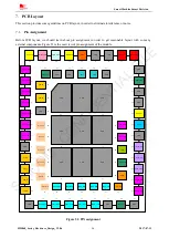
Страница 57: ...ETLIGHT SIM1_RST SIM1_CLK SIM1_DET SIM1_DATA BT_ANT SIM2_CLK SIM2_DET SIM2_DATA SIM2_RST SIM2_VDD UART2_TXD SPK1P VRTC MICP MICN USB_VBUS USB_DM GSM_ANT STATUS SIM1_VDD MCCA3 GND UART2_RXD GND GPS_RXD...

Страница 58: ...ner diode and capacitor should be placed close to VBAT pin The trace of pin 36 and pin37 to main GND should be as short and wide as possible 7 2 3 SIM Card Interface Ensure SIM card holder is far away...

Страница 59: ...digital interface pins GPIO and UART 8 2 Recommended Operating Conditions Table 35 Recommended operating conditions Symbol Parameter Min Typ Max Unit GSM_VBAT GSM power supply voltage 3 4 4 0 4 4 V G...

Страница 60: ...0 27 V 0 4 V VOH High level output voltage 1 62 V 2 7 V VOL Low level output voltage 0 36 V 0 4 V 8 5 SIM_VDD Characteristics Table 38 SIM_VDD characteristics Symbol Parameter Min Typ Max Unit VO Outp...

Страница 61: ...RS 3Rx 2Tx GSM850 EGSM900 DCS1800 PCS1900 323 340 212 236 mA mA mA mA Data mode GPRS 4Rx 1Tx GSM850 EGSM900 DCS1800 PCS1900 217 223 153 163 mA mA mA mA IMAX Peak current During Tx burst 2 0 A Note In...

Страница 62: ...cification requirement Table 42 GSM850 and EGSM900 conducted RF output power GSM850 EGSM900 PCL Nominal output power dBm Tolerance dB for conditions Normal Extreme 5 33 2 2 5 6 31 3 4 7 29 3 4 8 27 3...

Страница 63: ...the maximum power level the output power tolerance should not exceed 2dB under normal condition and 2 5dB under extreme condition 8 9 2 Module RF Receive Sensitivity Table 44 shows the module s condu...

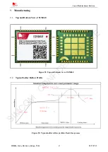
Страница 64: ...sign_V1 06 63 2017 07 13 9 Manufacturing 9 1 Top and Bottom View of SIM868 Figure 52 Top and bottom view of SIM868 9 2 Typical Solder Reflow Profile Figure 53 Typical solder reflow profile of lead fre...

Страница 65: ...processing IPC JEDEC J STD 033 must be followed 9 4 Baking Requirements SIM868 modules are vacuum packaged and guaranteed for 6 months storage without opening or leakage under the following conditions...

Страница 66: ...ware_Design_V1 06 65 2017 07 13 10 Packaging SIM868 module support tray packaging Figure 54 Packaging introduce Figure 55 Module tray drawing Table 48 Tray size Length 3mm Width 3mm Number 242 0 161 0...

Страница 67: ...re 56 Small carton drawing Table 49 Small Carton size Length 10mm Width 10mm Height 10mm Number 270 180 120 50 20 1000 Figure 57 Big carton drawing Table 50 Big Carton size Length 10mm Width 10mm Heig...

Страница 68: ...SMS and Cell Broadcast Service CBS 8 GSM 11 14 Digital cellular telecommunications system Phase 2 Specification of the SIM Application Toolkit for the Subscriber Identity Module Mobile Equipment SIM...

Страница 69: ...ted MS Mobile Station GSM part also referred to as TE MT Mobile Terminated PAP Password Authentication Protocol PBCCH Packet Broadcast Control Channel PCB Printed Circuit Board PCL Power Control Level...

Страница 70: ...avigation kbps Kilo bits per second MSL moisture sensitive level MSAS Multi Functional Satellite Augmentation System NMEA National Marine Electronics Association PRN Pseudo Random Noise Code QZSS Quas...

Страница 71: ...Your cellular terminal or mobile receives and transmits radio frequency energy while switched on RF interferes can occur if it is used close to TV sets radios computers or other electric equipment Roa...

Страница 72: ...71 2017 07 13 Contact us Shanghai SIMCom Wireless Solutions Co Ltd Address Building A SIM Technology Building No 633 Jinzhong Road Shanghai P R China 200335 Tel 86 21 3252 3300 Fax 86 21 3252 3020 UR...

Отзывы: