© 2021 SignalCore, Inc. All Rights Reserved
Hardware Manual
SC5319A & SC5320A
20 GHz to 40 GHz RF Downconverter
Preliminary Rev 0.1
www.signalcore.com
Страница 1: ...2021 SignalCore Inc All Rights Reserved Hardware Manual SC5319A SC5320A 20 GHz to 40 GHz RF Downconverter Preliminary Rev 0 1 www signalcore com...
Страница 2: ...upply Connection 10 Mini USB Connection 12 Reset Button Pin Hole 12 3 Functional Description 13 Overview 13 The Signal Chain 13 The RF Input 14 The LO Input Output 14 The Input Path Switch 14 The RF C...
Страница 3: ...Register 0x1B REFERENCE_ADJUST 25 Register 0x1C STORE_DEFAULT_STATE 26 Register 0x1D SELF_SYNTH_CAL 26 Register 0x1E DEVICE_STANDBY 26 Register 0x1F AUTO_CONV_PARAMS 27 Query Registers 27 Register 0x3...
Страница 4: ...RS232 5 PXI Express 5 Setting Up the PCI to Serial Bridge 5 Writing to the Device 6 Reading from the Device 6 6 Calibration 7 Calibration EEPROM Map 7 Conversion Gain 8 Absolute Gain of the RF Conver...
Страница 5: ...CUSTOMER S RIGHT TO RECOVER DAMAGES CAUSED BY FAULT OR NEGLIGENCE ON THE PART OF SIGNALCORE INCORPORATED SHALL BE LIMITED TO THE AMOUNT THERETOFORE PAID BY THE CUSTOMER SIGNALCORE INCORPORATED WILL NO...
Страница 6: ...s that do not infringe on the intellectual property rights of others SignalCore signalcore com and the phrase preserving signal integrity are registered trademarks of SignalCore Incorporated Other pro...
Страница 7: ...EMS HARDWARE AND OR SOFTWARE UNANTICIPATED USES OR MISUSES OR ERRORS ON THE PART OF THE USER OR APPLICATIONS DESIGNER ADVERSE FACTORS SUCH AS THESE ARE HEREAFTER COLLECTIVELY TERMED SYSTEM FAILURES AN...
Страница 8: ...l SignalCore products in their original antistatic bags Remove the product from its packaging and inspect it for loose components or any signs of damage Notify SignalCore immediately if the product ap...
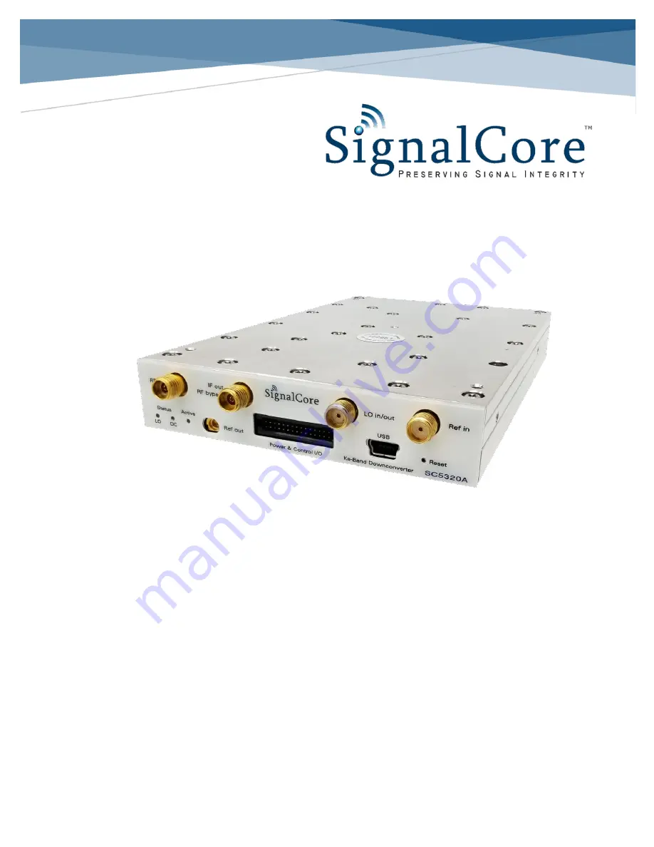
Страница 9: ...ector is an MMCX type Exercise caution when fastening cables to the signal connections it is important not to twist and turn the cable to tights on the K or SMA connectors rather the cables should be...
Страница 10: ...conversion LO is selected to use the internal synthesizer the synthesized signal is export out via this port otherwise this port takes an external source as the LO Ref In Out This is the 10 MHz refen...
Страница 11: ...8 H 10 00 SR is provided with the product The pin definitions are listed in Table 3 Pinouts are different for different SignalCore products with the same connector type Please ensure that mating conne...
Страница 12: ...2021 Rev 0 1 11 Physical Description Figure 4 Proper Removal of Latching Style Ribbon Connectors...
Страница 13: ...ing table PIN USB Function Description 1 VBUS Vcc 5 Volts 2 D Serial Data neg 3 D Serial Data pos 4 ID Not Used 5 GND Device Ground also tied to connector shell Reset Button Pin Hole Behind this pin h...
Страница 14: ...r has a single conversion stage that converts the RF signal to an intermediate frequency IF The RF input range of this downconverter is from 20 GHz to 40 GHz while the output IF range is from 50 MHz t...
Страница 15: ...as an output for the synthesized signal In other words the device can export its LO signal out to be used by other devices This is useful in phase coherent multiple channel systems that uses a common...
Страница 16: ...from its image A band select filter at the RF input port is recommended to properly filter through the signal of interest before down conversion The First Mixer and IF Path The mixer RF mixer of the d...
Страница 17: ...5 dB while the RF attenuator has resolution of 0 5 dB To set the downconverter for better sensitivity or better SNR the gain should be shifted to the RF input path of the device before the mixer The R...
Страница 18: ...d as the base clock by enabling the device to phase lock to it the device will only attempt to lock when the presence of a reference signal is detected at the input port This sets the device to phase...
Страница 19: ...the power and control interface block for the device All supply rails are produced on board their voltages are regulated and actively filtered to keep noise to a minimum Thus these downconverters are...
Страница 20: ...bytes is the sum of the register address 1 Byte and its corresponding data bytes For example to set the RF frequency value eight bytes must be written the sum of the 1 register byte and 7 data bytes S...
Страница 21: ...O_CONV_PARAMS 0x1F 7 0 Linear mode Linear mode Auto amp ctrl HW auto conv 15 8 IF level dB 7 0 23 16 Sign IF level dB 14 8 31 24 Mixer level dB 7 0 39 32 Sign Mixer level dB 14 8 47 40 RF level dB 7 0...
Страница 22: ...ed oscillator of LO1 Bytes written 2 Bytes read 1 Bits Type Name Width Description 1 0 WO Loop Gain 2 0 Low loop gain improves phase noise 50 kHz 1 Normal loop gain 2 High loop gain improves phase noi...
Страница 23: ...ed for PXIe and RS232 Register 0x12 LO_FREQUENCY This register sets the final IF value Bytes written 2 Bytes read 1 Bits Type Name Width Description 55 0 W Frequency word 56 Frequency word in Hz 7 0 R...
Страница 24: ...r 0x15 ATTENUATOR This register sets the value of the device attenuators Bytes written 4 Bytes read 1 Bits Type Name Width Description 7 0 W Attenuator value 8 In 0 25 dB LSB for IF 0 5 dB LSB for RF...
Страница 25: ...W IF enable 1 0 IF output is disabled signal is shunt to ground 1 If Output is enabled 7 1 W Not used 7 Set to zeros 7 0 R Read back byte 8 Read 1 byte back is required for PXIe and RS232 Register 0x1...
Страница 26: ...nal 10 MHz TCXO 1 W PXI10Enable 1 Only on SC5319A to enable export of the 10 MHz backplane clock this bit is ignored in the SC5320A 2 W REF Direction 1 Set the reference port SMA to as input or output...
Страница 27: ...n 2 Bytes read 1 Bits Type Name Width Description 0 W Oscillator Select 1 0 Coarse VCO 1 Sum VCO 7 1 W Used 7 EEPROM address 7 0 R Read back byte 8 Read 1 byte back is required for PXIe and RS232 Regi...
Страница 28: ...ice from changing frequencies due to heavy computation 7 6 W unused 2 Set to zeros 22 8 W Absolute IF level 15 IF level in dB steps 23 W Sign of IF level 1 0 positive 1 negative 38 24 W Absolute mixer...
Страница 29: ...ET_DEVICE_STATUS 0x32 7 0 Zeros 7 0 GET_DEVICE_INFO 0x33 7 0 Info SERIAL_OUT_BUFFER 0x34 55 0 Zeros 55 0 Register 0x30 GET_DEVICE_PARAM Write to this register the required device parameter to query fr...
Страница 30: ...ype Name Width Description 7 0 W Unused 7 Set to zeros 0 R Pll status LO1 SUM 1 The summing PLL of LO 1 R Pll status LO1 CRS 1 The coarse tuning PLL of LO 2 R Pll status LO1 FINE 1 The fine tuning PLL...
Страница 31: ...tput enabled 18 R Device_Accessed 1 Has software accessed opened the device 63 19 R Invalid data 46 Ignore Register 0x33 GET_DEVICE_INFO Write to this register to query the device information such as...
Страница 32: ...Q 2 U64 zeros Data Reserved 3 8 Reference DAC 9 U16 zeros zeros zeros zeros zeros zeros DAC value Signal Path 10 U16 zeros zeros zeros zeros zeros zeros Signal path Attenuators 11 U16 IF Atten RF Atte...
Страница 33: ...it Description 0 HW auto calculation state 1 Auto Preamp control 4 2 Linearity mode 7 5 Zero 14 8 IF level absolute value 15 IF level sign 22 16 Mixer level absolute value 23 Mixer level sign 30 24 RF...
Страница 34: ...vision Information The first 4 bytes represent the hardware revision and last 4 bytes represent the firmware revision of the device These 4 bytes encompass a 32 bit floating point number so the data n...
Страница 35: ...2021 SignalCore Inc All Rights Reserved Section 2 Communication Interfaces and Calibration...
Страница 36: ...1 Frequency is sent in 1000th of Hertz so the data that represents the frequency is 32 000 000 000 000 milli Hertz 2 This number can be represented by a 64 bit unsigned long and in Hexadecimal is 0x...
Страница 37: ...low for the entire duration of a register transfer Once a full transfer has been received the device will proceed to process the command and de assert low the SRDY pin The status of this pin may be m...
Страница 38: ...lly between 50 to 300 after reception Writing the SPI Bus The SPI transfer size in bytes depends on the register being targeted The first byte sent is the register address and subsequent bytes contain...
Страница 39: ...device communication control set is provided in the following table Table 9 RS232 Control Setting Baud rate Rate of transmission Data bits The number of bits in the data is fixed at 8 Parity Parity i...
Страница 40: ...vides the format details of the received data PXI Express The PXIe interface contains a high speed PCIe to Serial bridge chip This bridge chip communicates with the onboardmicrocontroller serially The...
Страница 41: ...needed for each device register The first byte sent is the device register address followed by the most significant byte of the register s associated data When a device register is fully written that...
Страница 42: ..._32 Temp coeffs band1 13 GHz 13Ghz band2 20GHz and band3 20 GHz c1 c2 c1 c2 c1 c2 0x398 50 200 Float_32 IF response cal frequencies 100 200 300 3500 in MHz 0x4B0 50 200 Float_32 IF3_response relative...
Страница 43: ...e applied to other relative configured states of the device The established reference state of the device is as follows All attenuators are set to 0 dB IF value is set at 2 GHz RF preamplifier is disa...
Страница 44: ...ver it must be corrected for frequency offset from 2000 MHz Thereare offset gain response valuesmeasured at 1500 MHz and 1600 MHz so a simple linear interpolation between 2 points should be sufficient...
Страница 45: ...Rev 0 1 SC5319A SC5320A Hardware Manual SignalCore Inc 10 SC5319A SC5320A Hardware Manual Revision Table Revision Revision Date Description 0 1 10 19 21 Document Created preliminary...