


41110555
Rev 1.0
November 01, 2017
32
Product Technical Specification
Detailed Interface Specifications
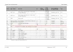
3.12. Clock Interface
The AirPrime HL77xx modules support two digital clock interfaces.
Enabling or disabling the clock out feature can be done using AT commands. For more information
about AT commands, refer to document [2] AirPrime HL77xx AT Commands Interface Guide.
Refer to the following table for the pad description of the clock out interfaces.
Table 26. Clock Interface Pad Description
Pad Number
Signal Name
I/O
I/O Type
Description
22
GNSS_FREQ_OUT
O
1.8V
26MHz Digital Clock output
23
32K_CLKOUT
O
1.8V
32.768kHz Digital Clock output
3.13. Debug Interface
The AirPrime HL77xx modules provide a 2-wire debug port interface.
Table 27. Software Trace Pad Description
Pad Number
Signal Name*
I/O*
I/O Type
Description
44
DEBUG_TX
O
1.8V
Debug Transmit Data
51
DEBUG_RX
I
1.8V
Debug Receive Data
*
According to module view.
Note:
It is strongly recommended to provide access through Test Points to this interface.
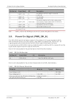
3.14. JTAG Interface
The JTAG interface provides debug access to the core of the AirPrime HL77xx modules. These JTAG
signals are accessible through solder-able test points.
Refer to the following table for the pad description of the JTAG interface.
Table 28. JTAG Pad Description
Pad Number
Signal Name
Function
236
JTAG_RESET
JTAG RESET
237
JTAG_TCK
JTAG Test Clock
238
JTAG_TDO
JTAG Test Data Output
239
JTAG_TMS
JTAG Test Mode Select
240
JTAG_TRST
JTAG Test Reset
241
JTAG_TDI
JTAG Test Data Input
Note:
It is recommended to provide access through Test Points to this interface the JTAG pads (for Failure
Analysis debugging). All signals listed in the table above should be outputs on the customer board to
allow JTAG debugging.


