


Semiconductor Group
105
On-Chip Peripheral Components
7.7
Watchdog Timer
As a means of graceful recovery from software or hardware upset a watchdog timer is provided in
the SAB 80(C)515/80(C)535. lf the software fails to clear the watchdog timer at least every
65532
µ
s, an internal hardware reset will be initiated. The software can be designed such that the
watchdog times out if the program does not progress properly. The watchdog will also time out if
the software error was due to hardware-related problems. This prevents the controller from
malfunctioning for longer than 65 ms if a 12-MHz oscillator is used.
The watchdog timer is a 16-bit counter which is incremented once every machine cycle. After an
external reset the watchdog timer is disabled and cleared to 0000H. The counter is started by
setting bit SWDT (bit 6 in SFR IEN1). After having been started, the bit WDTS (watchdog timer
status, bit 6 in SFR IP0) is set. Note that the watchdog timer cannot be stopped by software. lt can
only be cleared to 0000H by first setting bit WDT (IEN0.6) and with the next instruction setting
SWDT. Bit WDT will automatically be cleared during the second machine cycle after having been
set. For this reason, setting SWDT bit has to be a one cycle instruction (e.g. SETB SWDT). This
double instruction clearing of the watchdog timer was implemented to minimize the chance of
unintentionally clearing the watchdog. To prevent the watchdog from overflowing, it must be cleared
periodically.
Starting the watchdog timer by setting only bit SWDT does not reload the WDTREL register to the
watchdog timer registers WDTL/WDTH. A reload occurs only by using the double instruction refresh
sequence SETB WDT / SETB SWDT.
lf the software fails to clear the watchdog in time, an internally generated watchdog reset is entered
at the counter state FFFCH, which lasts four machine cycles. This internal reset differs from an
external reset only to the extent that the watchdog timer is not disabled. Bit WDTS (was set by
starting WDT) allows the software to examine from which source the reset was initiated. lf it is set,
the reset was caused by a watchdog timer overflow.
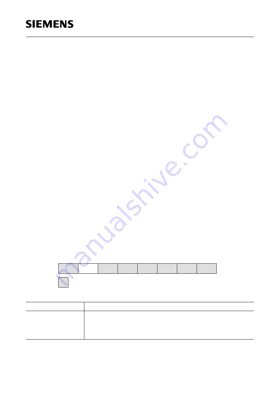
Figure 7-45
Special Function Register IEN0
Bit
Function
WDT
Watchdog timer refresh flag.
Set to initiate a refresh of the watchdog timer. Must be set directly before
SWDT is set to prevent an unintentional refresh of the watchdog timer.
WDT is reset by hardware two processor cycles after it has been set.
These bits are not used by the watchdog timer.
0AFH 0AEH 0ADH 0ACH 0ABH 0AAH 0A9H
0A8H
EAL
WDT
ET2
ES
ET1
EX1
ET0
EX0
0A8H
IEN0
*
Содержание SAB 80515 Series
Страница 9: ...Semiconductor Group 9 Introduction Figure 1 2 Block Diagram ...
Страница 12: ...Semiconductor Group 12 Fundamental Structure Figure 2 1 Detailed Block Diagram ...
Страница 18: ...Semiconductor Group 18 Central Processing Unit Figure 3 1 Fetch Execute Sequence ...
Страница 22: ...Semiconductor Group 22 Memory Organization Figure 4 3 Mapping of the Lower Portion of the Internal Data Memory ...
Страница 30: ...Semiconductor Group 30 External Bus Interface Figure 5 1 a and b External Program Memory Execution ...
Страница 38: ...Semiconductor Group 38 On Chip Peripheral Components Figure 7 3 Output Driver Circuits of Ports 1 through 5 ...
Страница 59: ...Semiconductor Group 59 On Chip Peripheral Components Figure 7 16 a Functional Diagram Serial Interface Mode 0 ...
Страница 60: ...Semiconductor Group 60 On Chip Peripheral Components Figure 7 16 b Timing Diagram Serial Interface Mode 0 ...
Страница 61: ...Semiconductor Group 61 On Chip Peripheral Components Figure 7 17 a Functional Diagram Serial Interface Mode 1 ...
Страница 62: ...Semiconductor Group 62 On Chip Peripheral Components Figure 7 17 b Timing Diagram Serial Interface Mode 1 ...
Страница 73: ...Semiconductor Group 73 On Chip Peripheral Components Figure 7 25 A D Converter Block Diagram ...
Страница 83: ...Semiconductor Group 83 On Chip Peripheral Components Figure 7 33 a Timer 2 Block Diagram ...
Страница 111: ...Semiconductor Group 111 On Chip Peripheral Components Figure 7 54 Timing Diagram System Clock Output ...
Страница 113: ...Semiconductor Group 113 Interrupt System Figure 8 1 a Interrupt Structure of the SAB 80 C 515 80 C 535 ...
Страница 114: ...Semiconductor Group 114 Interrupt System Figure 8 1 b Interrupt Structure of the SAB 80 C 515 80 C 535 cont d ...
Страница 204: ...Semiconductor Group 204 Instruction Set XCH A Ri Operation XCH A Ri Bytes 1 Cycles 1 Encoding 1 1 0 0 0 1 1 i ...
Страница 215: ...Device Specifications Semiconductor Group 215 ...
Страница 217: ...Device Specifications Semiconductor Group 217 Pin Configuration P LCC 68 ...
Страница 219: ...Device Specifications Semiconductor Group 219 Logic Symbol ...
Страница 226: ...Device Specifications Semiconductor Group 226 Figure 1 Block Diagram ...
Страница 229: ...Device Specifications Semiconductor Group 229 Figure 2 Memory Address Spaces ...
Страница 239: ...Device Specifications Semiconductor Group 239 Figure 4 Block Diagram of the A D Converter ...
Страница 241: ...Device Specifications Semiconductor Group 241 Figure 5 Interrupt Request Sources ...
Страница 242: ...Device Specifications Semiconductor Group 242 Figure 6 Interrupt Priority Level Structure ...
Страница 268: ...Device Specifications Semiconductor Group 268 AC Testing Input Output Waveforms AC Testing Float Waveforms ...