


Semiconductor Group
6-56
1999-04-01
On-Chip Peripheral Components
C541U
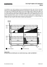
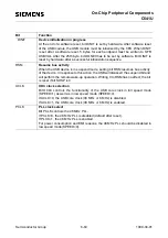
The data transfers between USB memory and the CPU are handled via the SFR USBVAL. With a
CPU write access to USBVAL, the value written into it is transferred to the USB memory location
which is defined by the content of the endpoint specific endpoint base address register EPBAn and
the content of the address offset register ADROFF. At USB memory read accesses from the CPU
the data is transfered in reverse direction.
A write operation to USBVAL is only successfull if either DIR=0 and CBF=1 (write operation) or
DIR=1 and CBF=0 (read operation).
Sequence of two or more write operations to USBVAL register using move-immediate instruction is
unsupported. It is recommended to use either accumulator or a temporary register for storing an
immediate data, before writing it to USBVAL register.
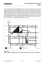
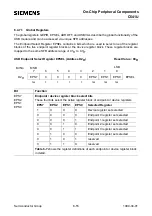
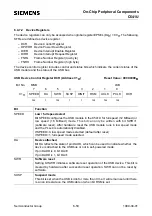
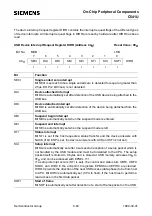
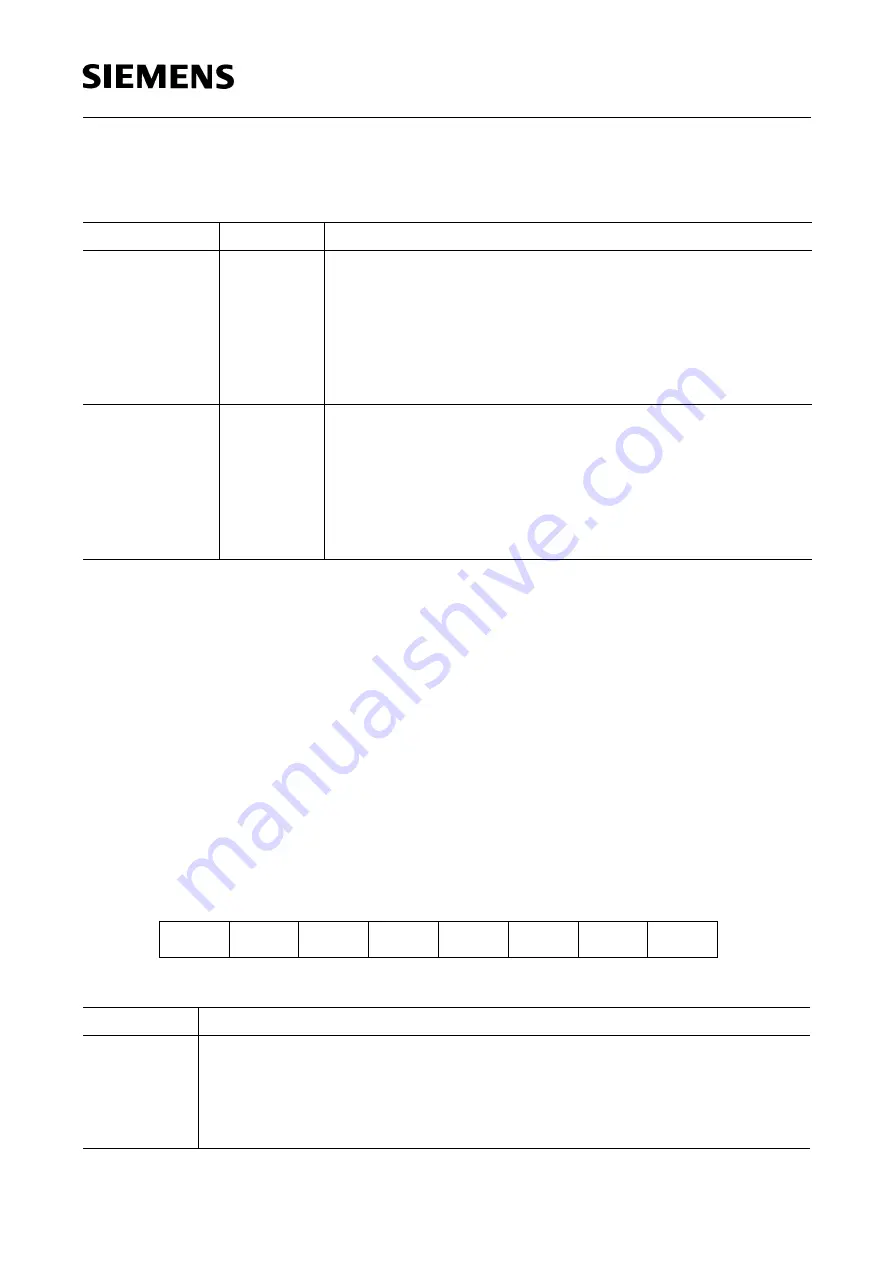
USB Data Register USBVAL (Address D3H)
Reset Value : 00H
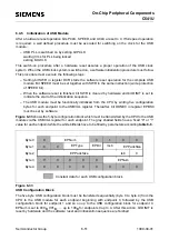
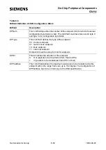
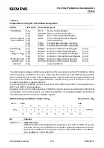
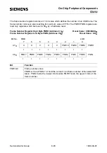
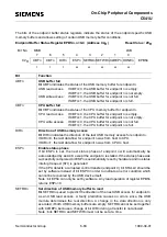
Table 6-7
Endpoint/Device Register Set Address Assignment
EPSEL
SFR Addr.
Selected Register
1XXXXXXXB
(Device register
block selected)
C1H
C2H
C3H
C4H
C5H
C6H
C7H
DCR
: Device Control Register
DPWDR: Device Power Down Register
DIER
: Device Interrupt Enable Register
DIRR
: Device Interrupt Request Register
reserved address
FNRL
: Frame Number Register (low byte)
FNRH : Frame Number Register (high byte)
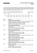
0XXXXnnnB
(nnn =
000B to 100B)
(Endpoint nnnB
register block
selected)
C1H
C2H
C3H
C4H
C5H
C6H
C7H
EPBCn : Endpoint n Buffer Control Register
(n=0-4)
EPBSn : Endpoint n Buffer Status Register
(n=0-4)
EPIEn : Endpoint n Interrupt Enable Register
(n=0-4)
EPIRn : Endpoint n Interrupt Request Register (n=0-4)
EPBAn : Endpoint n Base Address Register
(n=0-4)
EPLENn: Endpoint n Buffer Length Register
(n=0-4)
reserved address
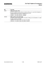
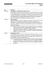
Bit
Function
USBVAL.7-0
USB data value
USBVAL stores the 8-bit data byte during transfers from CPU to USB memory and
from USB memory to CPU. Bit NOD in the EPIRn register indicates when the CPU
processes an USBVAL read operation with an empty USB buffer or a USBVAL
write operation to a full USB buffer.
MSB
LSB
USBVAL
.7
.6
.5
.4
.3
.2
.1
.0
7
6
5
4
3
2
1
0
Bit No.
rw
rw
rw
rw
rw
rw
rw
rw
D3H
Содержание C541U
Страница 1: ... 8 LW 026 0LFURFRQWUROOHU 8VHU V 0DQXDO http www siem ens d Sem iconductor ...
Страница 7: ......
Страница 21: ...Semiconductor Group 2 6 1997 10 01 Fundamental Structure C541U ...
Страница 37: ...Semiconductor Group 4 6 1997 10 01 External Bus Interface C541U ...
Страница 133: ...Semiconductor Group 6 88 1999 04 01 On Chip Peripheral Components C541U ...
Страница 163: ...Semiconductor Group 8 8 1997 10 01 Fail Safe Mechanisms C541U ...
Страница 185: ...Semiconductor Group 10 14 1997 10 01 OTP Memory Operation C541U ...
Страница 192: ...Semiconductor Group 12 7 Index C541U ...


