


UX-P115U
5 – 3
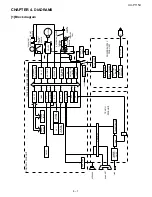
2.2.12 Video Processing
The CX06835 supports two modes of shading correction for scanner
data non-uniformity arising from uneven sensor output or uneven illu-
mination. Corrections are provided on either an 8-pixel group or are
applied separately to each pixel. Dark level correction and gamma cor-
rection are also provided.
Two-dimensional Error Diffusion/Dithering is performed on halftone
images.
The CX06835 includes an 8 x 8 dither table, which is programmable
and stored internally (8-bit per table entry). The table is arranged in a
matrix of 8 rows by 8 columns. The video processing circuit provides
mixed-mode detection/processing and multi-level Resolution Conver-
sion for the scanner multi-level data. The conversion ratio of the multi-
level Resolution Conversion is fixed to B4-A4 conversion.
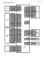
2.2.13 Operator Panel Interface
Operation Panel functions are supported by the operator output bus
OPO[6:0], the operator input bus OP[3:0], and two control outputs
(LCDCS and LEDCTRL).
The CX06835 can directly interface to a 28-key keypad.
A 2-line LCD display module with 20 characters per line can be sup-
ported.
2.2.14 Synchronous Serial Interface (SSIF)
One or optionally two Synchronous only Serial Interfaces (SSIF) are
built into the CX06835, which allows it to communicate with external
peripherals. Each SSIF provides separate signals for Data (SSTXD,
SSRXD), Clock (SSCLK), and Status (SSSTAT). Each SSIF is a
duplex, three-wire system. The SSIF may be configured to operate as
either a master or a slave interface. The bit rate, clock polarity, clock
phase, and data shifting order are programmable.
2.2.15 Synchronous/Asynchronous Serial Interface
(SASIF)
One or optionally two Synchronous/Asynchronous Serial Interface
(SASIF) performs the following:
• Serial-parallel conversion of data received from a peripheral
device.
• Parallel-to-serial conversion of data for transmission to a peripheral
device.
This interface consists of serial transmit data (SASTXD), serial receive
data (SASRXD), and a serial clock (SASCLK). The SASIF includes a
programmable bit rate generator for asynchronous and synchronous
operations. The data shifting order, data bit number, and the SASCLK
polarity are programmable.
The optional SASIF 2 has an additional pin called DSS_AVAIL. This
signal can be used to tristate the SASCLK2 and SASTXD2 signals.
2.2.16 Real Time Clock (RTC)
The CX06835 includes a battery backup real time clock. The RTC will
automatically maintain the proper date and time for 32 years. Leap
year compensation is included. A 32.768 kHz or 65.536 kHz crystal is
required by the RTC.
2.2.17 Tone Generator (ALT_TONE)
The CX06835 provides a programmable tone generator output. The
frequency of the tone generator is programmable from 400 Hz to 4
kHz. By using a PWM programmable high frequency as a modulation
frequency, the output level can be made programmable.
2.2.18 Watchdog Timer
The Programmable Watchdog Timer is intended to guard against firm-
ware lockup on the part of either executive-controlled background
tasks or interrupt-driven tasks, and can only be enabled by a sequence
of events under control of the Watchdog Control Logic. Once the
Watchdog Timer has been enabled, it can not be disabled unless a
system reset occurs.
2.2.19 Reset and Power Control
The RESETn I/O pin provides an internally generated reset output to
external circuits, or it can accept an externally generated reset signal.
This reset signal will not reset the RTC. Separate RTC battery power
inputs are provided for battery-backup functions. A BATRSTn pin is
provided, which resets the RTC circuits and other SCC circuits.
2.2.20 Power Up/Down Control
Power Up/Down detection is provided internally. The threshold volt-
ages are:
• Power Up detection level = 2.83V to 2.95V.
An internally generated power down signal controls internal switching
between primary and battery power. This control signal is also pro-
vided as an output on the PWRDWNn pin. An externally generated
power down detector (optional) can be provided as an input on the
PWRDWNn pin by setting the INTPWRDWNEn pin.
2.2.21 Stand-by and Sleep Modes
Two power saving modes are provided to reduce the power consump-
tion. In stand-by mode, the CPU is functional, but the modem clock is
turned off to save power. When this occurs, the modem may be acti-
vated by software under different conditions. In sleep mode, the clock
is cut off from both the modem and the CPU to increase the power
savings.
The system can be activated by paper insertion, key pressing events,
and telephone ring detection.
2.2.22 Embedded Modem DSP
The embedded modem DSP is a synchronous 9600 bps half-duplex
modem with error detection and DTMF generation/reception. It pro-
vides data transmission/reception from regular PSTN lines, PBX, or
private lines.
The modem can operate at any standard V.29 data speed up to 9600
bps as well as in V.21 and V.23 modes.
The modem is designed for use in Group 3 facsimile machines. It sat-
isfies the requirements specified in ITU-T recommendations V.29,
V.27ter, V.21 Channel 2, and T.4 , and meets the signaling require-
ments of T.30. It also performs HDLC framing according to T.30 at all
speeds.
NOTE: For technical details, refer to the FM209/FM214 Designer’s
Guide, (document 1175).
2.2.23 Software and Firmware Support Features
Available software and embedded firmware provides the following:
• Modem support for speeds up to 9600 bps.
• ECM under conditional assembly.
• DRAM memory support under conditional assembly.
• MH, MR and MMR support.
• Page memory receiving.
• 5 ms minimum scan line time.
• Conditional Error Diffusion or Dither table (8x8) support.
• Dark Level Correction support.
• Single motor support.
• 28-key operator panel support.
• Call progress support for Europe and U.S.A.
• Monochrome inkjet print engine support.
Содержание UX-P115
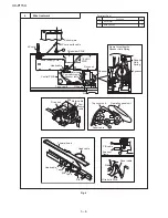
Страница 60: ...UX P115U 6 7 7 Control PWB parts layout Top side ...
Страница 61: ...UX P115U 6 8 8 Control PWB parts layout Bottom side ...
Страница 63: ...UX P115U 6 10 2 TEL LIU PWB parts layout Top side The TEL LIU PWB of the model employs lead free solder ...
Страница 64: ...UX P115U 6 11 3 TEL LIU PWB parts layout Bottom side The TEL LIU PWB of the model employs lead free solder ...
Страница 66: ...UX P115U 6 13 2 Power supply PWB parts layout Top side 3 Power supply PWB parts layout Bottom side ...
Страница 76: ...UX P115U 8 5 MEMO ...