


UX-P115U
5 – 2
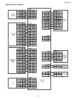
[2] Circuit description of control PWB
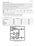
1. General description
Fig. 2 shows the functional blocks of the control PWB, which is com-
posed of 3 blocks.
2. Description of each block
2.1. Main control block
The main control block is composed of CONEXANT 1 chip fax engine
(SCE209), FLASH (2Mbit), DRAM (4Mbit).
Devices are connected to the bus to control the whole unit.
2.1.1 SCE209 (IC3): pin-176 QFP (FAX CONTROLLER)
1 chip fax engine has Internal Integrated Analog (20438) and Internal
memory (SRAM: 32kbit).
2.1.2 SST39VF020P (IC1): pin-32 TSOP (FLASH)
FLASH of 2Mbit equipped with software for the main CPU.
2.1.3 IS41LV85125 (IC2): pin-28 SOJ (DRAM)
Image memory for recording process.
Memory for recording pixel data without paper.
2.2. IC3 (SCE209) Hardware description
2.2.1 Integrated Controller (SCC)
The Controller contains an internal MC24 Processor with a 16-MB
address space and dedicated circuitry optimized for facsimile image
processing and monitoring and for thermal or thermal transfer printer
support.
The CPU provides fast instruction (up to 10 MHz clock speed) execu-
tion and memory efficient input/output bit manipulation. The CPU con-
nects to other internal functions over an 8-bit data bus and 24-bit
address bus and dedicated control lines.
The 24-bit external address bus, 8-bit data bus, control, status and
decoded chip select signals support connection to external ROM,
SRAM, DRAM, and FLASH memory.
2.2.2 DRAM Controller
The CX06835 includes a DRAM controller with signal and page mode
access support which supports fast, normal, or slow refresh time.
DRAM memory space is provided in one block up to 4 MB. A maxi-
mum of 4 MB of DRAM is supported. This space has a programmable
size and starting address. Refresh is performed automatically and is
supported in stand-by mode. CAS and RAS signal support is provided
for one-DRAM banks for both 4-bit and 8-bit organizations. Access
speeds from 50ns to 70ns can be supported.
2.2.3 DMA Channels
Six internal DMA channels support memory access for scanner, T.4/
T.6, and resolution conversion. DMA Channel 2 can be reprogrammed
for external access to thermal printing, thermal transfer, or plain paper
inkjet printing.
2.2.4 External RAM and ROM
Moveable and programmable size external SRAM memory of up to 1
MB, DRAM memory of up to 4 MB, and ROM of up to 2 MB can be
directly connected to the SCE209. By using an external address
decoder, the size of SRAM and/or ROM can be extended. The ROM
stores all the program object code.
2.2.5 Flash Memory Controller
The SCE209 includes a flash memory controller that supports NOR,
NAND, and Serial NAND-type flash memory. The supported size of
NOR-type memory is up to 1 MB and the supported size of NAND-type
memory is unlimited.
2.2.6 Stepper Motor Control
Eight outputs are provided to external current drivers: four to the scan-
ner motor and four to the printer motor. The stepping patterns are pro-
grammable and selectable line times are supported. A timeout circuit
controls the power control of the motors. The printer or scanner motor
outputs can be programmed as GPOs for applications using single
motor or paper printers.
2.2.7 T.4/T.6 Compression/Decompression
MH, MR and MMR compression and decompression are provided in
hardware. T.4 line lengths of up to 8192 pixels are supported. MMR
and Alternating Compression/Decompression (ACD) on a line by line
basis provide support for up to three independent compression and
decompression processes.
2.2.8 Bi-level Resolution Conversion
One independent programmable bi-level 1D-resolution conversion
block is provided to perform expansion or reduction on the T.4 decom-
pressed data and scan image data. Image expansion can be pro-
grammed up to 200% and reduction down to 33%. Vertical line O-Ring
and data output bit order reversal is also provided.
2.2.9 Printer IF
The Printer Interface provides a standard connection between the
SCE209 and a thermal printhead to support thermal printing or thermal
transfer. The thermal printer interface consists of programmable data,
latch, clock, and up to four strobe signals. Programmable timing sup-
ports traditional thermal printers, as well as the latchless split mode
printers, and line lengths of up to 2048 pixels. Line times from 5 ms to
40 ms are supported.
The SCE209 includes a thermal ADC (TADC) function utilizing a D/A
converter and a comparator to monitor the printhead temperature.
External terminating resistors must be supplied; the values are deter-
mined by the specific printhead selected.
As an option, plain paper inkjet printing can be supported.
2.2.10 TPH Hardware Timer
The TPH hardware timer provides a 500 ms timer that can be re-trig-
gered or reset.
2.2.11 Scanner and Video Control
Five programmable control and timing signals support common CCD
and CIS scanners. The video control function provides signals for con-
trolling the scanner and for processing its video output. Three pro-
grammable control signals (START, CLK1n, and CLK2) provide timing
related to line and pixel timing. These are programmable with regard
to start time, relative delay and pulse width.
Two video control output signals (VIDCTL[1:0]) provide digital control
for external signal pre-processing circuitry. These signals provide a per
pixel period, or per line period, timing with programmable polarity con-
trol for each signal.
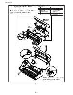
Fig. 2 Control PWB function block diagram
(1) SCE209
IA(CX20438)
MEMORY(SRAM)
(2) FLASH
(3) DRAM
Содержание UX-P115
Страница 60: ...UX P115U 6 7 7 Control PWB parts layout Top side ...
Страница 61: ...UX P115U 6 8 8 Control PWB parts layout Bottom side ...
Страница 63: ...UX P115U 6 10 2 TEL LIU PWB parts layout Top side The TEL LIU PWB of the model employs lead free solder ...
Страница 64: ...UX P115U 6 11 3 TEL LIU PWB parts layout Bottom side The TEL LIU PWB of the model employs lead free solder ...
Страница 66: ...UX P115U 6 13 2 Power supply PWB parts layout Top side 3 Power supply PWB parts layout Bottom side ...
Страница 76: ...UX P115U 8 5 MEMO ...