background image


 MANUAL


PHOTO: 


GENERAL
Power source 

Speakers:

Output power:

Semiconductors:

Dimensions: Width;

Height;
Depth;

Weight:

In the interests of user-safety the set should be

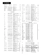
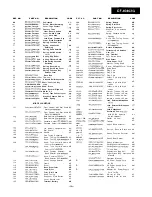
restored to its original condition and only parts
identical to those specified be used.

For the mechanical adjustment, refer to the

 Service Manual 

 already

issued.

SPECIFICATIONS

(AC operation)

R M S ;  

 (3W   3W) (DC 

A C   1  

  a n d  

tion, 10% distortion)

4 Transistors

 Diodes


 6”)

DC 


 or 

 type   6)

98mm 
3.1 kg (6.8 

 without batteries


 woofer   2

Ceramic type tweeter   2
PMPO; 


   8W)

(AC operation)

M P O ;   1 2 W  


TAPE RECORDER
Tape 

Compact cassette tape

Frequency response:


Signal/noise ratio:

45dB

Input sensitivity and impedance:

External mic.;

600 ohms

Loaded impedance:

Headphones;

8 ohms   25 ohms

R A D I O
Frequency range:

F M ;   8 7 . 6   M H z  


  M H z

AM; 526.5 

 1605.5 

   2.3 MHz 

 7.3 MHz

SW2   7.3 MHz 

 22.0 MHz

Specifications for this model are subject to change without
prior notice.

Содержание GF-4949ZG

Страница 1: ... IOV 127V and 22OV 24OV tion 10 distortion 5 ICS 4 Transistors 50 60Hz 11 Diodes 2 LEDs 445mm 17 l 2 233 5mm 9 3 l 6 DC 9V UM SUM 1 or R20 type x 6 98mm 3 7 8 3 1 kg 6 8 tbs without batteries 12cm 4 3 4 woofer x 2 Ceramic type tweeter x 2 PMPO 16W BW 8W AC operation MPO 12W 6W 6W TAPE RECORDER Tape Compact cassette tape Frequency response 50Hz 10 OOOHz Signal noise ratio 45dB Input sensitivity and...

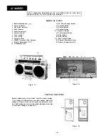
Страница 2: ...ly Socket 1 1 14 Cassette Holder i 15 Record Button 16 Rewind Button 17 Playback Button 18 Fast forward Button 19 Stop Button 20 Eject Button 21 Beat Cancel Switch 22 External Microphone Jacks 23 Battery Compartment Lid Figure 2 l Figure 2 2 VOLTAGE SELECTION Before operating the unit on mains check the preset voltage If the voltage is different from your local voltage adjust the voltage as follow...

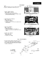
Страница 3: ...he mechanism block can be removed Figure 3 l q MAIN P W B REMOVAL Refer to Figure 3 3 1 Remove eight screws 0 2 Remove the LED P W B from two stoppers Then the main P W B can be removed from the back cabinet POWER P W B REMOVAL Refer to Figure 3 3 1 Remove two screws 0 2 Disconnect one socket Figure 3 3 DIAL CORD STRINGING 1 Turn the drum fully clockwise and stretch its cord over the parts in the ...

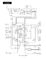
Страница 4: ...0 SH SH f I i r r Figure 4 BLOCK DIAGRAM 4 ...

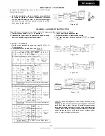
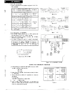
Страница 5: ... S CY TING IF Connect instruments as shown in Figure 5 2 RF Connect instrumentsas shown in Figure 5 3 4 output A M 600 600 kHz kHz L7 Track 5 A M ing 1400 1400 kHz kHz TC5 6 Repeat steps 2 3 4 and 5 until no further Improvement can be made RF Connect instruments as shown in Figure 5 4 2 25 LOW Band MHz end of L9 dial cover age 7 4 High end of TC7 MHz Adjust for dial maximum I A n I OUtDUt c 110 SW...

Страница 6: ...QUENCY ALIGNEMNT l Set the Band Selector Switch SWI to FM position and Function Switch SW102 to stereo position l Before this adjustment connect the anode side of Stereo Indicator D103 to GND l As shown in Figures 6 3 and 6 4 connect instruments FREQUENCY DIAL AD JUST POINTER MENT REMARKS 98MHz 54dB 98MHz VRl Adjust for unmodulated 38 f O lSkHz To Telescopic Rod Antenna 2 5 ohm Rl 37 5 ohm R2 75 O...

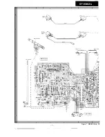
Страница 7: ...FJ IWO ANTEtwM 1 M A I N P W B 1 A 1 zj 1 I 2 3 I 4 I 5 I 6 A B C D E F G n 1 I 2 I 3 I 4 I 5 I 6 I Figure 7 WIRING SIDE OF 7 _ _ _ __ _ _ __ _ ___ _ i ...

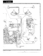
Страница 8: ...6 I 7 I 8 I 9 I 10 I 11 I 12 I I I SWITCH P W B 6 I 7 I 8 I 9 I 10 I 11 I 12 IG SIDE OF P W B O A R D 8 ...

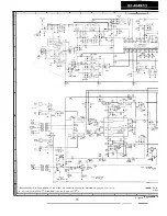
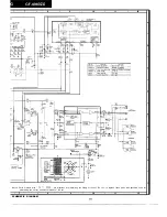
Страница 9: ...AK B I A S OX t Specifications or wiring diagrams of this model are subject to change for improvement without prior notice l N O T ES ON SC EMATIC DIAGRAM can be found on Page 6 1 I 2 I 3 I 4 I 5 Notes Parts maint I 6 I F i g u r e 9 SCHEMATII 9 ...

Страница 10: ...lsGR RIPPLE FILTER Notes Parts marked with 1 are important for maintaining the safety of the set Be sure to replace these parts with specified ones for _ maintaining the safety and pertormance ot the set I 7 I 8 I 9 I 10 I 11 I 12 1 SCHEMATIC DIAGRAM ...

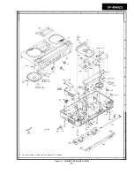
Страница 11: ...1 I 2 I 3 I 4 I 5 I 6 SP203R ch SP204L ch MAIN P W B l The parts without number are not supplied for servicing I I 1 1 J I 4 I 9 I 0 Figure 11 CABINET EXPLODED VIEW ll ...

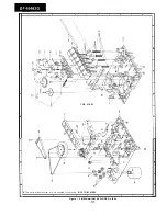
Страница 12: ...A 8 C D E F G H 1 I 2 I 3 I 4 I 5 I 6 TOP VIEW 0 The parts without number are not supplied for servicing BOTTOM VIEW 1 I 2 I 3 I 4 I 5 I 6 Figure 12 MECHANISM EXPLODED VIEW 12 ...

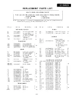
Страница 13: ...M Oscillator Bias Oscillator 560pH Noise Suppressor 47pH Noise Suppressor TRANSFORMERS Tl T2 RCI LIOI 57AFZZ FM IF RCILl0312AFZZ FM Detector RCILl03lOAFZZ AM IF 92LPT 277A Power AC AC A A AC A D AP t AC A B A D I AC AW REF NO CFl CF3 VCl 2 vc3 4 TCl 2 TC4 7 1 v c 5 TC3 TC5 TC6 TC8 VRl VRlOl VR103 PART NO DESCRIPTION CODE FILTERS R Fl LF0080AFZZ Ceramic FM IF 10 7MHz A D RFI LA0074AFZZ Ceramic AM I...

Страница 14: ...Semiconductor O OlZMFD 25V lO Semiconductor A A 68OPF 5OV 10 Ceramic 0 0056MFD 25V lo Semiconductor 68OPF 5OV lo Ceramic O O012MFD 25V lO Semiconductor REF NO C131 132 PART NO VCTYPUl EX823K Cl36 VCKZPUl HF102Z C203 204 VCTYPUl EX393K C207 208 VCTYPUl EX102K DESCRIPTION CODE O O82MFD 25V lo AB Semiconductor O OOlMFD 5OV 80 20 A A Ceramic O O39MFD 25V lO A A Semiconductor 0 001 MFD 25V lO A A Semic...

Страница 15: ...1978 S w i t c h R e c o r d P l a y b a c k A K 92LSWICH 197C Switch Function Selector A M 110 92LLID277A 92LPINT277A 92LMEC277HNLOl 92LSUPT799A 92LKNOB220A 92LKNOB244A 92LKNOB220B J201 so501 SW501 1 SP20 1 202 SP203 204 SW1 A F SW101 A JI SW1 02 A FI SW1 03 A B C SW104 92LKNOB244B 111 92LKNOB220C GSWS0267AFZZ QSW FOI 58AFZZ 92LP CASE279A 92LP CASE294A 92LP AD277A 92LBAG277A 92LBAG117A 92LKNOB244...

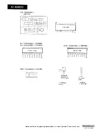
Страница 16: ...18 10 rnnnnnng TOP VIEW r L 1 LlLJUUU J 9 IClOl VHIM51544L 1 M51544L FRONT VIEW n nV 000 000 EC8 2SC945 AP 2SC945 AK 2SC1815 GR u 1 2 fat 5 GL 9PR25 Red E EMITTER C COLLECTOR 1 ANODE 6 BASE 2 CATHODE Writer and Editor Engineering Administration of Audio Systems Group Sharp Corp A8310 1554YM K 1 Printed in Japan ...

Отзывы: