background image

-

CE-l29P

NOTES:

Some of tape recorders may not operate properly owing
to different

specification or electrical characteristies

affected by signal distortion, electrical noise, level drop-
out caused after long years of use.

• When using the tape recorder fitted with the mixing

feature, it needs to disable the mixing function for both
recording and playback_

Oepending on the

tape

recorder used, better reading

result may be attained when the red plug is unplugged
from the MIC [ack,

As it may impede proper data transfer and verification
depending on the position of the volume control, tone

control, bass control, and treble control, try to find the

optlrnum

level by varying their positions.

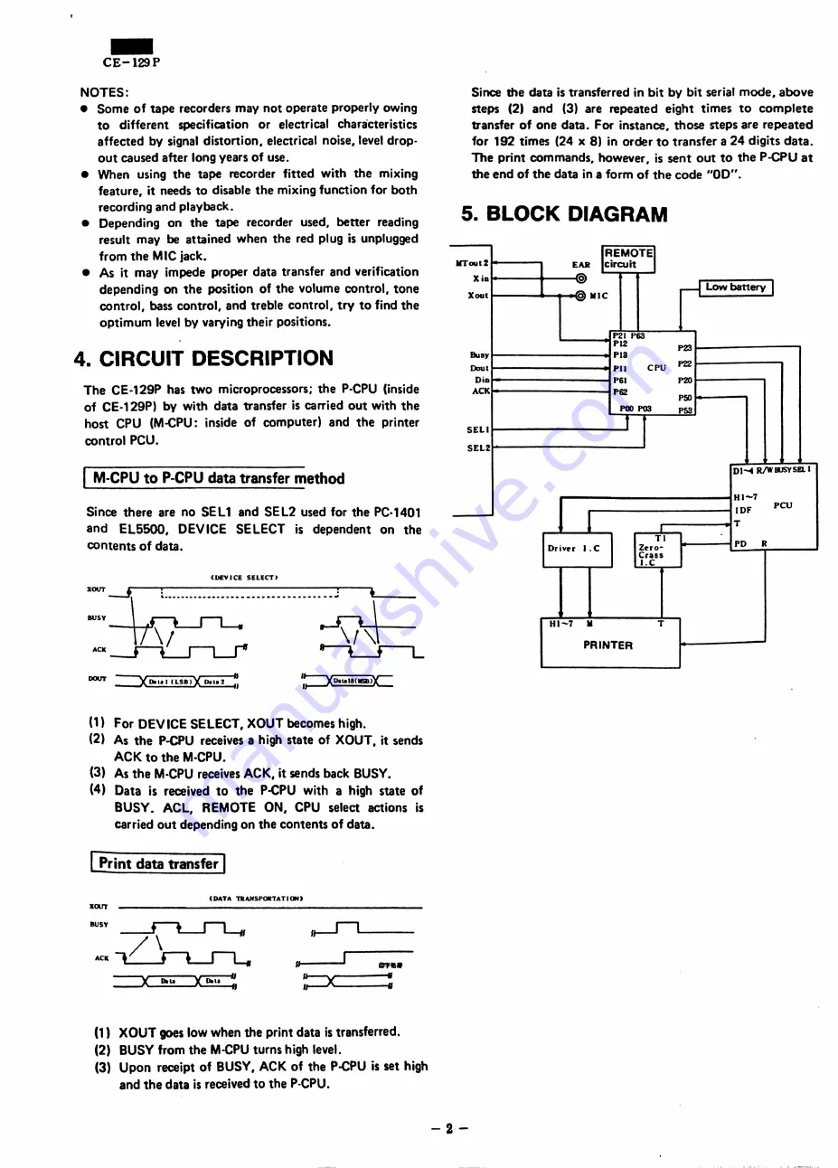
4. CIRCUIT DESCRIPTION

The CE-129P has two microprocessors; the P-CPU (inside

of CE-129P) by with data transfer is carried out with the
host CPU (M-CPU: inside of computer) and the prlnter

control PCU.

I

M-CPU to P-CPU data transfer method

Since there are no SEl1 and SEl2 used for the PC-1401
and

El5500,

OEVICE SElECT

is dependent on the

contents of data.

(UEVICE

SELECTJ

DOUT

(11

For OEVICE SElECT, XOUT becomes high.

(2) As the P-CPU receives a high state of XOUT, it sends

ACK to the M-CPU.

(3) As the M-CPUreceives ACK, it sends back BUSY.
(4) Oata is received to the P-CPU with a high state of

BUSY. ACl,

REMOTE ON, CPU select actions is

carried out depending on the contents of data.

[print data transfer

I

(DATA

DAHSPORTATlorrn

XOUT

IUSY

~

ACK

/

\

~

IIIY ••

(1) XOUT goes low when the print data is transferred.
(2) BUSY from the M-CPUturns high level.

(3) Upon receipt of BUSY, ACK of the P-CPU is set high

and the data is received to the P-CPU.

Since the data is transferred in bit by bit serial mode, above
steps (2) and (3) are repeated eight times to complete
transfer of one data, For instance, those steps are repeated
for 192 times (24 x 8) in order to transfer a 24 digits data.

The print commands, however, is sent out to the P-CPU at

the end of the data in a form of the code "00".

5. BLOCK DIAGRAM

lfToulZ

I~EM.OTEI

I

EAR

CIl"CU

it

XiD

"&'

~

r-I

Low

battery

J

Xoal

-"'" IIIC

-

P21 P&3

PI2

P23

BuS)"

PlI

Ooul

Pli

CPU

P22

DiD

PSI

P20

ACK

P62

P50

POO P03

P53

SELI

, I

SELZ

D I.... RIW JIJSY

sn

I

HI-1

IDF

PCU

T

TI

I

PD

R

Drivrr

I. C

Z~ro-
Crn.

I.C

HI-1

11

T

PRINTER

-2-

Do not sale !

Содержание CE-129P

Страница 1: ... and Operation manual Paper feed speed Paper Power source Operation Power consumption Operating temperature Dimensions Weight Accessories MODEL CE 129P Printer Cassette Interface 3 TAPE RECORDER INTERFACING METHOD CE I29P Tape recorder Tepe R order CE 129P I 1 tI I I I I Grey ptug tr nsftr nd eDU liDnl BI kplug bemoll contral kpl I troll Grey pI transfer and ClDUalionl Red plug racordingl i c sett...

Страница 2: ... is dependent on the contents of data UEVICE SELECTJ DOUT 11 For OEVICE SElECT XOUT becomes high 2 As the P CPU receives a high state of XOUT it sends ACK to the M CPU 3 As the M CPUreceivesACK it sends back BUSY 4 Oata is received to the P CPU with a high state of BUSY ACl REMOTE ON CPU select actions is carried out depending on the contents of data print data transfer I DATA DAHSPORTATlorrn XOUT...

Страница 3: ...22 P53 04 Input Output Oata bus line between the P CPU and the PCU 23 POO SEL1 Input Select input signal It is not used in the PC 1400 El 5500 series 24 P40 VOO Input Output Setting VOO 4 6V 25 NC 28 NC 29 P41 l B Input Output low battery detection signal Normal high P42 VOO Input Output Setting VOO 4 SV VOO VOO Power supply VOO 4 6V 32 NC 33 GNO GNO Power supply OV 34 P43 GNO Input Output Setting...

Страница 4: ...of the motor 26 28 TSl 3 In Test pins 29 VP1 Out Printer control circuit supply power 30 32 BCl 3 ln Out PCU frequency controI 33 CCK Out Clock test pin 34 l fA In I Print density adjust pin _ JA and JB pin connection Notused I 35 HB I 36 HC In varies according to the printhead rank 37 38 Cl1 2 In Basic clock pulse control resistor fitting pin 39 PF In Paper feed key input 40 NP In GNO Connected 4...

Страница 5: ...operly connected in a manner as des cribed in Table 1 The VR should necessarily be set to the position mentioned in Fig 1 If set too much counterciockwise it may damage the printhead which mayaiso cause dot omission VR J FiS_ 5 Ensure before the operation of the oscilloscope that the time axle control knob is set at CALIBRATION Adjust the print density in the fOllowing sequence step 1 thru step 5 ...

Страница 6: ...rmal ICurrent check during printing I t Connect a computer to the CE 129P circuit 2 Supply 5 0V from stabilized oe power supply tp Vp line GND OV standard 3 Set the power switches in the computer and the CE 129P to ON to execute check program 1 IDEE Ä N z o z w o w a u 6 CE l29P Print sampIe 444444444444444444444444 444444444444444444444444 444444444444444444444444 444444444444444444444444 4444444...

Страница 7: ... CE l29P 9 CIRCUIT DIAGRAM l_ _L l_ D e äl I w r It r r 1 1 r I L CI N N N N N 10 I 0 i l o D u uv Ö e CI er E ID i i t It Ilr I J ID r u CD r Do not sale ...

Страница 8: ...I oe xc I 111 10 Jl r Z a LL 8 O o t u N C 0 N I N XI a lI I Ö E GI l er L I I 1 I I I I I I I 1 I t t JMt 0 S c z 0 I 1 SI 0 O 8 N 2 N E 10 10 f 1 L 6 o CL U U J CI I I UI 1 r 8 x _ t u t ID Do not sale ...

Страница 9: ...10 MAIN P W B I 1 11 10 ä ci ci z z g 0 z _ Do not sale ...

Страница 10: ... CE l29P Do not sale ...

Страница 11: ... CE l29P 11 SUB P W B I i n 111 Ir 11 Do not sale ...

Страница 12: ...12 PARTS LIST GUIDE l 1 eJ 31 I I A 32 3 _____ 12 _ _ Do not sale ...

Страница 13: ...CZI AH C Filter ESD H 14B 10 RRlYZ2400QCZZ AP B Relav II VCEAGUIAW107M AB C Capacitor_ lOWV l00uF 12 VCEAGU1AW108M AC C Capacitor lOWV l000 13 VCTYPUIEX472M AA C Capacitor 25WV 4700pf 14 VHDDS1588l2 1 AB B Diode DSI588l2 15 VHD10EIN 1 AB B Diode lOEIN 16 VHEHZ7A3 1 AB B Zener diode HZ7A3 17 VRD ST2EY391J AA C Resistor l 4W 3900 5 18 VRD ST2EY681J AA C Resistor 1 4W 6800 5 l 19 VRD ST2EY682J AA C R...

Страница 14: ... Z I 5 0 5 C C Z Z 18I G F T A 2 1 C C Z Z IBatterv terminal B IBatterv terminal Lr _N_ AA icrew C2 6X6 AA I 1 AC I _N ll Main PWB unit NQI PARTS CODE DESCRIPTION I PSPAPI230CCZZ _2_ Q C N w i 3 0 8 C C A i JQulrlnter 8_pin plack 3IQSW K I n 5CCll RC CZI021CCZZ RC CZI03ICCZZ RC CZI035CCZZ Dt _ 7In IIt t 77 _p_1 _ 1 B 1 _l _I i 1Spacer PJlpeI Jeee switch A apacitor CI 1lF lOOOpF J QQ2 apaCllor 470p...

Отзывы: