16
AK - 44
CHASSIS
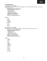
8. Not connected
9. Not connected
10. Symmetrical IF output 1
11. Symmetrical IF output 2
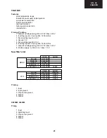
Band switching table:
Pin 3
Pin 4
Pin 5
Low band
0 V
0 V
+ 5 V
Mid band
0 V
+ 5 V
0 V
High band + 5 V
0 V
0 V
General description of UV1316
The UV1316 tuner belongs to the UV 1300 family of tuners, which are designed to meet a wide range of applications.
It is a combined VHF, UHF tuner suitable for CCIR systems B/G, H, L, L’, I and I’.
Features of UV1316
Member of the UV1300 family small sized UHF/VHF tuners
Systems CCIR: B/G, H, L, L’, I and I’; OIRT: D/K
Digitally controlled (PLL) tuning via I²C-bus
Off-air channels, S-cable channels and Hyper-band
World standardized mechanical dimensions and world standard pinning
Complies to “CENELEC EN55020” and “EN55013”
Pinning, Pin Value
1. Gain control voltage (AGC): 4.0 V, Max: 4.5 V
2. Tuning voltage
3. I²C-bus address select: Max: 5.5 V
4. I²C-bus serial clock :Min: -0.3 V, Max: 5.5 V
5. I²C-bus serial data :Min: -0.3 V, Max: 5.5 V
6. Not connected
7. PLL supply voltage: 5.0 V, Min: 4.75 V, Max: 5.5 V
8. ADC input
9. Tuner supply voltage: 33 V, Min: 30 V, Max: 35 V
10. Symmetrical IF output 1
11. Symmetrical IF output 2
General description of UV1336
UV1336 series is developed for reception of channels broadcast in accordance with the M, N standard.
Features of UV1336
Global standard pinning
Integrated Mixer-Oscillator & PLL function
Conforms to CISPR 13, FCC and DOC (Canada) regulations
Low power consumption
Both Phono connector and ‘F’ connector are available
Pinning, Pin Value
1. Gain control voltage: 4.0 V, Max: 4.5 V
2. Tuning voltage
3. Address select Max: 5.5 V
4. Serial clock: Min: -0.3 V, Max: 5.5 V
5. Serial data :Min: -0.3 V, Max: 5.5 V
6. Not connected
7. Supply voltage: 5.0 V, Min: 4.75 V, Max: 5.5 V
8. ADC input (optional)
9. Tuning supply voltage: 33 V, Min: 30 V, Max: 35 V
10. Ground
11. IF output
Содержание 21LT-45SES
Страница 6: ...6 21LT 45S CHASSIS LAYOUT Mother Unit CRT Unit ...
Страница 44: ...32 AK 44 CHASSIS 18 2 Schematic Diagram of Video Circuit 1 I H G F E D C B A 2 3 4 5 6 7 Page 33 ...
Страница 45: ...33 AK 44 CHASSIS 8 9 10 11 12 13 14 I H G F E D C B A Page 32 18 2 Schematic Diagram of Video Circuit ...
Страница 46: ...34 AK 44 CHASSIS 1 I H G F E D C B A 2 3 4 5 6 7 Page 35 18 3 Schematic Diagram of SMPS Circuit ...
Страница 47: ...35 AK 44 CHASSIS 8 9 10 11 12 13 14 I H G F E D C B A Page 34 18 3 Schematic Diagram of SMPS Circuit ...
Страница 48: ...36 AK 44 CHASSIS 1 I H G F E D C B A 2 3 4 5 6 7 18 4 Schematic Diagram of Audio Circuit ...
Страница 49: ...37 AK 44 CHASSIS 8 9 10 11 12 13 14 I H G F E D C B A 18 5 Schematic Diagram of Deflection Circuit ...
Страница 50: ...38 AK 44 CHASSIS 1 I H G F E D C B A 2 3 4 5 6 7 Page 39 18 6 Schematic Diagram of Scart AV Front Circuits ...
Страница 52: ...40 AK 44 CHASSIS 1 I H G F E D C B A 2 3 4 5 6 7 18 7 Schematic Diagram of CRT Socket Circuit ...
Страница 55: ...43 AK 44 CHASSIS Notes ...


