


5
PROTECT SELECT
PROTECT SELECT OEM
Operating instructions
Multifunctional safety controller
EN
Proximity switches with Reed contacts (e.g. safety switches
such as the Schmersal BNS type series) may not be
connected to inputs (I0, I4, I12, I14) due to the alternative
function as signalling output. They must satisfy the following
technical requirements
– switching capacity: min. 240 mW
– switching voltage: min. 24 VDC
– switching current: min. 10 mA
When a safety mat is connected make sure that the clock
outputs are decoupled, for example via diodes.
When installing the cables the safe analogue inputs
AI0 / AI1 high frequency signal decoupling must be avoided.
Recommended cable type for the safe analogue inputs AI0 /
AI1: LAPP KABEL unitronic® FD CP (TP) plus 1 x 2 x 0.75
For inputs that are configured for antivalent (1NO/1NC)
evaluation, the NO contact must always be connected to the
input with the odd number.
With single-channel use the input with the odd number is
not used.
When connecting safety door interlocks the door position
should be connected to the even input and magnet position
connected to the odd input.
4.5 Actuator level
2 x safe p-/n-switching semiconductor outputs (Q0/Q0N, Q1/Q1N)
with 24 VDC
2 x safe p-switching semiconductor outputs (Q2, Q3) with 24 VDC
2 x safe relay outputs (QR1, QR2) with common supply (QR0)
up to 250 VAC or 24 VDC
4 x operational optional message outputs (Y0 … Y 3) with 24 VDC
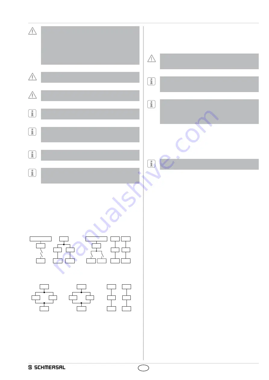
Relay outputs
250 V / 24 V
GND
GND
QR 2
K 1
K 2
QR 1
QR 2
* 1
250 V / 24 V
GND
GND
QR 1
QR 2
K 1
K 2
QR 0
QR 1
QR 2
Semi-conductor
outputs
K 2
Q 0N
Q 0
K 1
* 1
K 2
Q 1 N
Q 1
K 1
* 1
GND
GND
Q 2
Q 3
K 1
K 2
*1 Measures for short circuit shutout against the supply are necessary
Test pulses
The correct function of the semi-conductor outputs is secured by a
cyclical test, i.e. all switched outputs are deactivated for approx. 0.5 ms
(in the event of capacitive loads the deactivation is for a maximum of 2
ms).
If contactors and coils are connected suitable protective
measures (free-wheeling diode, varistor or similar) must be
taken to protect the internal output switching.
If after a shutdown of max. 2 ms no HIGH signal is detected
on the semiconductor output (e.g. due to a capacitive load),
a system failure is the result.
If a subsequent assembly is disturbed by the test pulse
it can be eliminated by including a D/C filter in the circuit:
Typical values: 3…10 kΩ,
1000 nF
10…30 kΩ,
330 nF
The resulting signal delay is to be considered.
Signalling outputs
The terminals I0/Y0, I4/Y1, I12/Y2 and I14/Y3 may be used both as
safe input and as signalling output.
Which function is used will depend on the application program
(see chapter 8.1).
The signalling outputs Y0…Y3 are not safety-related.


