


CP3005 – User Guide Rev. 1.8
// 45
4.3.3.
Control Register 0 (CTRL0)
The Control Register 0 holds a series of bits defining general/common configuration functions.
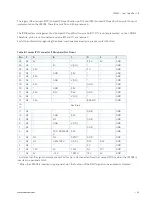
Table 21: Control Register 0 (CTRL0)
Address
0x282
Bit
7
6
5
4
3
2
1
0
Name
VGAM
R/W
01
BFUS
Reserved
R
00000
Access
R/W
Reset
0
Bitfield
Description
7 - 6
VGAM
DESCRIPTION
7 - 6
VGAM
VGA mode configuration:
00 = Automatic VGA front detection
01 = Front VGA (uEFI BIOS default)
10 = Rear VGA
11 = VGA disabled
5
BFUS
SPI boot flash selection:
0 = Select the standard SPI boot flash for update
1 = Select the recovery SPI boot flash for update
4.3.4.
Control Register 1 (CTRL1)
The Control Register 1 holds a series of bits defining general/common configuration functions.
Table 22: Control Register 1 (CTRL1)
Address
0x283
Bit
7
6
5
4
3
2
1
0
Name
SRST
VRST
TRST
CRST
Res
SCOMA
Res
Res
Access
R/W
R
R/W
R/W
R
R/W
R
R
Reset
1
1
1
0
0
not avai-
lable*
0
0
* Reset value is depending on the board version ordered. Default is low (0), when CP3005 Rear I/O version is ordered.
But when a CP3005 front version is ordered, an automatic switch over to the 8HP extension module is processed per
default.
Bitfield
Description
7
SRST
SATA Flash module configuration:
0 = Reset of SATA Flash module
1 = SATA Flash module running
6
VRST
Integrated processor graphics controller configuration:
0 = Processor graphics controller disabled
1 = Processor graphics controller enabled
5
TRST
Trusted Platform Module (TPM) configuration:
0 = TPM disabled