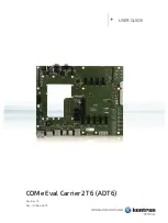
background image

 

USER GUIDE 


COMe Eval Carrier2 T6 (ADT6) 

Doc. Rev 1.2 

Doc.-ID: 1065-4472 


Содержание Kontron COMe Eval Carrier2 T6

Страница 1: ...USER GUIDE COMe Eval Carrier2 T6 ADT6 Doc Rev 1 2 Doc ID 1065 4472...

Страница 2: ...COMe Eval Carrier2 T6 ADT6 User Guide Rev 1 2 Page left intentionally blank www kontron com 2...

Страница 3: ...ation will be suitable for the specified use without further testing or modification Kontron expressly informs the user that this user guide only contains a general description of processes and instru...

Страница 4: ...vide adequate design and operating safeguards You are solely responsible for compliance with all legal regulatory safety and security related requirements concerning your products You are responsible...

Страница 5: ...t page of this user guide or visit our website CONTACT US Customer Support Find Kontron contacts by visiting http www kontron com support Customer Service As a trusted technology innovator and global...

Страница 6: ...ailure to observe the precautions indicated and or prescribed by the law may endanger your life health and or result in damage to your material Please refer also to the High Voltage Safety Instruction...

Страница 7: ...voltages before performing any work on this product Earth ground connection to vehicle s chassis or a central grounding point shall remain connected The earth ground cable shall be the last cable to b...

Страница 8: ...are present their temperature restrictions must be taken into account In performing all necessary installation and application operations only follow the instructions supplied by the present user guid...

Страница 9: ...for the environmental impact of their products especially when the product become waste Encourage separate collection and subsequent treatment reuse recovery recycling and sound environmental disposal...

Страница 10: ...COM Express Documentation 15 1 5 COM Express Benefits 15 2 System specifications 16 2 1 Component Main Data 16 2 2 Block diagram 17 2 3 Product Variants 18 2 4 Environmental Conditions 18 3 Mainboard...

Страница 11: ...3 Product Variants 18 Table 4 Environmental Conditions 18 Table 5 1000Base T connector 22 Table 6 Signals 22 Table 7 USB Double Connector 23 Table 8 Graphic Interfaces 23 Table 9 Graphic Interfaces DD...

Страница 12: ...Connector 23 Figure 8 HD Audio 25 Figure 9 HD Audio 10 pin 26 Figure 10 GPIO 28 Figure 11 Configuring GPIO Pins using JIDA32 K Station 28 Figure 12 Feature Connector with 24 pins 29 Figure 13 Externa...

Страница 13: ...uge variety of interfaces Main purpose of this carrier board is to bring out all the signals from COM Express connector of COMe Type6 modules to industry standard interfaces The key features are 1x 10...

Страница 14: ...e cXX modules are Kontron s COM Express modules in compact form factor 95 mm x 95 mm COMe eXX modules are Kontron s COM Express modules in extended form factor 155 mm x 110 mm The COMe Eval Carrier2 T...

Страница 15: ...les The baseboard designer can optimize exactly how each of these functions implements physically Designers can place connectors precisely where needed for the application on a baseboard designed to o...

Страница 16: ...S3 S4 S5 GPIO GPIO Header with 10 pins I2C Feature Connector J57 Battery CR2032 battery holder Fan 4 pin fan connector Voltage can be 5 V or 12 V default 4 pole Carrier Board Power Power input Carrier...

Страница 17: ...COMe Eval Carrier2 T6 ADT6 User Guide Rev 1 2 www kontron com 17 2 2 Block diagram Figure 2 Block Diagram COMe Type6 Eval Carrier...

Страница 18: ...Components and materials of the product must not contain lead mercury cadmium hexavalent chromium polybrominated biphenyls PBB or polybrominated diphenyl ethers PBDE Directive 2002 95 EC RoHS II Comp...

Страница 19: ...ower Connector J99 3 eDP J14 4 ATX Power Connector J5 5 LVDS J2 6 Button Switches 7 4x PCI x1 J81 J82 J83 J84 8 POST Code Display 9 PCIe x16 10 4x SATA 11 2x COMe J61 12 HDA J48 13 GPIO J49 14 SPI J45...

Страница 20: ...T6 ADT6 User Guide Rev 1 2 www kontron com 20 3 2 Front panel Figure 4 Front Panel 23 5x Audio Connectors J78 24 2x DP J32 25 1x DP J39 26 2x USB J63 27 4x USB 3 0 28 1x GE Connector J33 29 2x USB 24...

Страница 21: ...COMe Eval Carrier2 T6 ADT6 User Guide Rev 1 2 www kontron com 21 4 Mechanical Specification 4 1 Dimensions The dimensions of the carrier board are 244 0 mm x 305 0 mm Figure 5 Board Dimensions...

Страница 22: ...00Base T connector Pin Signal Ethernet 10 BaseT 100BaseT Gigabit Ethernet 1 MDI0 TX DA 2 MDI0 TX DA 3 MDI1 RX DB 4 MDI1 DC 5 MDI2 DC 6 MDI2 RX DB 7 MDI3 DD 8 MDI3 DD Table 6 Signals LED Signal 1 Off N...

Страница 23: ...ottom USB0 USB_SS0 J64 Top USB1 USB_SS1 J65 Bottom USB2 USB_SS2 J65 Top USB3 USB_SS3 J33 Bottom USB4 J33 Top USB5 J63 Bottom USB6 J63 Top USB7 Intel starts counting USB Ports with 1 while COMe Specifi...

Страница 24: ...N LVDS_I2C_CK LVDS_BKLT_EN LVDS_I2C_DAT LVDS_BKLT_CTRL EDP_HPD LVDS_VDD_EN LVDS_BKLT_EN LVDS_BKLT_CTRL 5 1 3 1 VGA J17 Table 11 Graphic Interfaces VGA Signal Pin HDSUB 15 Description I O Comment VGA_R...

Страница 25: ...input Lime Analog line level audio output for the main stereo signal front speakers or headphones Pink Analog microphone audio input Orange Analog line level audio output for center channel speaker a...

Страница 26: ...ble 14 HD Audio internal Pin Connector 1 HDA_BITCLK 4 HDA_SDIN1 5 HDA_SDIN0 6 HDA_SDIN2 8 HDA_SYNC 9 HDA_SDOUT 10 HDA_RST 5 1 6 COM Ports Table 15 COM Ports COMe Signal EC kCPLD function SER0_TX po_ua...

Страница 27: ...clkbuffer U12 FPGA U12 SMB_CLK Pin 13 B5 SMB_CLK_S0_CKBUF M10 SMB_DAT Pin 12 B6 SMB_CLK_S0_CKBUF L10 SMB_Alert Pin 10 J8 5 1 8 PCIe Slots J25 J81 J88 The slot for PCI Express Graphics is J25 with up...

Страница 28: ..._GPO0 P3 GPIO_GPI0 P4 GPIO_GPO1 P5 GPIO_GPI1 P6 GPIO_GPO2 P7 GPIO_GPI2 P8 GPIO_GPO3 P9 GPIO_GPI3 P10 GND Figure 11 Configuring GPIO Pins using JIDA32 K Station The GPI and GPO pins can be configured u...

Страница 29: ...l P1 V_5V0_S0 P2 GPO P3 BATLOW P4 GPI P5 SYS_RESET P6 WDT P7 LPC_SERIRQ P8 NC P9 I2C_DAT P10 SMB_ALERT P11 I2C_CLK P12 SMB_DAT P13 SMB_CLK P14 NC P15 WAKE P16 V_3V0_RTC P17 THRM P18 GND P19 PWR_OK P20...

Страница 30: ...0_S5 P19 V_3V3_S5 P20 V_1V8_S5 P21 V_12V0_S0 P22 V_5V5_S0 P23 V_3V3_S0 P24 V_1V5_S0 5 1 13 Fan 3 Pin 4 Pin Jumper J93 Figure 14 Fan 3 Pin 4 Pin Jumper with 3 pins J93 Jumpered to 2 3 Regulated 3 Pole...

Страница 31: ...ion 1 GND 2 V_Fan Power 12V 5V switchable 3 FAN_TACH_CON sense 4 FAN_PWM_CON drive 5 1 15 24 pin ATX Power connector J5 Figure 16 ATX Power connector with 24 pins Table 23 ATX Power connector with 24...

Страница 32: ...up time all the supply voltages should be shut down and left OFF for a time long enough to allow the internal board voltages to discharge sufficiently If the OFF time is not observed parts of the boa...

Страница 33: ...Input Current should be measured this should be done at this place 5 1 17 SPI BIOS J45 SOIC8 Socket J45 for external BIOS Flash Table 25 SPI BIOS COMe Signal Description SPI_CS SPI_CS logic implemente...

Страница 34: ...w kontron com 34 5 1 18 LPC eSPI J29 Close J66 for 1V8 eSPI mode 0pen J66 for 3V3 LPC mode Figure 18 LPC eSPI J29 Table 27 LPC eSPI J29 COMe Connector Pin LPC_AD 0 3 14 13 11 12 LPC_FRAME 24 LPC_DRQ 0...

Страница 35: ...rews for 5mm connectors 38017 0000 00 0 COMe Mount KIT 8mm 1set Mounting Kit for 1 module including screws for 8mm connectors Product Number Cables Description 96079 0000 00 0 KAB HSP 200mm Cable adap...

Страница 36: ...ication If any of the supply voltages drops below the allowed operating level longer than the specified hold up time all the supply voltages should be shut down and left OFF for a time long enough to...

Страница 37: ...ng the de assertion of the shutdown signal 2 Simultaneously with the leading edge of shutdown the 12 V main input power to the module is removed and these input power pins are externally clamped to gr...

Страница 38: ...for all signals for example ATX power signals share one power good Table 30 LEDs LED Signal Description D39 V_5V0_S5_ATX Power LED D8 V_5V0_S5 D7 V_3V3_S5 D48 V_12V0_S0 D50 V_5V0_S0 D49 V_3V3_S0 D9 P...

Страница 39: ...ble UART0 default Measure SER0 J13 Enable UART0 default Measure SER0 J72 Enable UART1 default Enable CAN Measure SER1 J73 Enable UART1 default Enable CAN Measure SER1 J11 Connect 3V0 RTC to module def...

Страница 40: ...run at Single Supply Mode this Jumper has to be removed Jumpers V_WIDE_MOD If these two Jumpers are closed the Wide Range input Voltage J99 is provided to the Com Express Module If these Jumpers are...

Страница 41: ...T6 ADT6 User Guide Rev 1 2 www kontron com 41 8 5 Button Switches Figure 20 Button Switches Table 32 Buttons Button Switch Function SW1 Powerbutton SW2 Sys_Reset SW3 Rapid Shutdown optional SW4 Sleep...

Страница 42: ...he wires have the right diameter to withstand the maximum available current the enclosure of the peripheral device fulfills the fire protection requirements of IEC EN60950 Table 33 Pin out List Pin Ro...

Страница 43: ...0_TX SATA1_TX DDI1_PAIR6 DDI1_CTRLDAT A_AUX 17 SATA0_TX SATA1_TX RSVD 10 18 SUS_S4 SUS_STAT ESPI_R ESET RSVD 10 19 SATA0_RX SATA1_RX PCIE_RX6 PCIE_TX6 20 SATA0_RX SATA1_RX PCIE_RX6 PCIE_TX6 21 GND FIX...

Страница 44: ...D FIXED GND FIXED GND FIXED 42 USB2 USB3 DDI3_PAIR1 DDI2_PAIR1 43 USB2 USB3 DDI3_PAIR1 DDI2_PAIR1 44 USB_2_3_OC USB_0_1_OC DDI3_HPD DDI2_HPD 45 USB0 USB1 RSVD 10 46 USB0 USB1 DDI3_PAIR2 DDI2_PAIR2 47...

Страница 45: ...EG_RX5 PEG_TX5 70 GND FIXED GND FIXED GND FIXED GND FIXED 71 LVDS_A0 LVDS_B0 PEG_RX6 PEG_TX6 72 LVDS_A0 LVDS_B0 PEG_RX6 PEG_TX6 73 LVDS_A1 LVDS_B1 GND GND 74 LVDS_A1 LVDS_B1 PEG_RX7 PEG_TX7 75 LVDS_A2...

Страница 46: ...3 95 SPI_MOSI VGA_I2C_CK PEG_RX13 PEG_TX13 96 TPM_PP VGA_I2C_DAT GND GND 97 TYPE10 SPI_CS RSVD 10 98 SER0_TX RSVD 10 PEG_RX14 99 SER0_RX RSVD 10 PEG_RX14 100 GND FIXED GND FIXED GND FIXED GND FIXED 10...

Страница 47: ...not be held responsible for any loss or damage caused to the equipment received without an RMA number The buyer accepts responsibility for all freight charges for the return of goods to Kontron s desi...

Страница 48: ...shock and ESD protection Goods returned to Kontron Europe GmbH in non proper packaging will be considered as customer caused faults and cannot be accepted as warranty repairs 4 Include the RMA Number...

Страница 49: ...ontroller sideband interface PCIe PCI Express PICMG PCI Industrial Computer Manufacturers Group POR Power On Reset PSU Power Supply Unit RTC Real Time Clock S0 ACPI OS System State 0 Indicates fully o...

Страница 50: ...rd products and tailor made solutions based on highly reliable state of the art embedded technologies Kontron provides secure and innovative applications for a variety of industries As a result custom...

Отзывы: