USER GUIDE
www.kontron.com
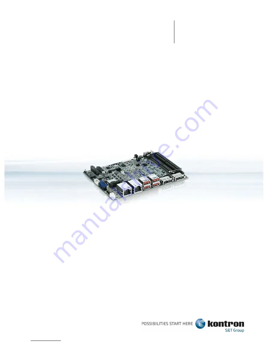
3.5"-SBC-WLU
Doc. User Guide, Rev. 1.8
Doc. ID: [To be Determined]
Страница 1: ...USER GUIDE www kontron com 3 5 SBC WLU Doc User Guide Rev 1 8 Doc ID To be Determined...
Страница 2: ...3 5 SBC WLU User Guide Rev 1 8 www kontron com 2 This page has been intentionally left blank...
Страница 3: ...suitable for the specified use without further testing or modification Kontron expressly informs the user that this user guide only contains a general description of processes and instructions which...
Страница 4: ...ly at your risk To minimize the risks associated with your products and applications you should provide adequate design and operating safeguards You are solely responsible for compliance with all lega...
Страница 5: ...w kontron com terms and conditions For contact information refer to the corporate offices contact information on the last page of this user guide or visit our website CONTACT US Customer Support Find...
Страница 6: ...scribed by the law may endanger your life health and or result in damage to your material ESD Sensitive Device This symbol and title inform that the electronic boards and their components are sensitiv...
Страница 7: ...before performing any work on this product Earth ground connection to vehicle s chassis or a central grounding point shall remain connected The earth ground cable shall be the last cable to be discon...
Страница 8: ...oduct then re pack it in the same manner as it was delivered Special care is necessary when handling or unpacking the product See Special Handling and Unpacking Instruction Quality and Environmental M...
Страница 9: ...Environmental Conditions 18 3 4 Standards and Certifications 18 3 5 Processor Support 20 3 6 System Memory Support 20 3 6 1 Memory Operating Frequencies 20 3 7 On board Graphics Subsystem 21 3 8 Powe...
Страница 10: ...Mode Selection JP10 63 8 BIOS 64 8 1 Starting the uEFI BIOS 64 8 2 Starting the uEFI BIOS 65 8 2 1 Main Setup Menu 65 8 2 2 Advanced Setup Menu 67 8 2 3 Power Setup Menu 83 8 2 4 Boot Setup Menu 85 8...
Страница 11: ...signment JP9 63 Table 45 Pin Assignment JP10 63 Table 46 Hotkeys Table 64 Table 47 Main Setup Menu Sub Screens and Functions 65 Table 48 List of Acronyms 89 List of Figures Figure 1 System Block Diagr...
Страница 12: ...Screen System Data and Time 66 Figure 41 BIOS Advanced Menu 68 Figure 42 BIOS Advanced Menu Display Configuration 69 Figure 43 BIOS Advanced Menu Super IO Configuration 71 Figure 44 BIOS Advanced Men...
Страница 13: ...SBC WLU board s special features and is not intended to be a standard PC AT textbook New users are recommended to study the short installation procedure stated in the following chapter before switchin...
Страница 14: ...ower supply unit shall comply with the requirements as defined in IEC 62368 1 according Clause 6 2 2 to power source category PS2 Limited Power Source 2 Insert the DDR4 2400 2133 module s Be careful t...
Страница 15: ...Explosionsgefahr bei unsachgem em Austausch der Batterie Ersatz nur durch denselben oder einen vom Hersteller empfohlenen gleichwertigen Typ Entsorgung gebrauchter Batterien nach Angaben des Herstell...
Страница 16: ...3 5 SBC WLU User Guide Rev 1 8 www kontron com 16 3 System Specifications 3 1 System Block Diagram Figure 1 System Block Diagram 3 5 SBC WLU...
Страница 17: ...eader 1x Mic in by header Network Connection Ethernet 2x GbE LAN RJ45 on rear Intel I219 LM Intel I210 AT Peripheral Connection USB 4x USB 3 2 Gen 2 Type A on rear 4x USB 2 0 by header Serial Port 2x...
Страница 18: ...the following environmental conditions It is the customer s responsibility to provide sufficient airflow around each of the components to keep them within the allowed temperature range Table 2 Environ...
Страница 19: ...WLU User Guide Rev 1 8 www kontron com 19 EN 61000 4 6 2013 EN 61000 4 8 2009 EN 61000 4 11 2004 A1 2017 FCC Class B FCC CFR Title 47 Part 15 Subpart B Class B ICES 003 Issue 6 2016 Class B ANSI C63...
Страница 20: ...C WLU has two DDR4 SO DIMM sockets The sockets support the following memory features 2x DDR4 SO DIMM 260 pin Dual channel with 1x SO DIMM per channel Up to 64 GB SPD timing supported ECC not supported...
Страница 21: ...guration Table 6 Three displays Configurations Display 1 Display 2 Display 3 Max Resolution Px at 60 Hz Display 1 Display 2 Display 3 LVDS DP DP 1920 x 1200 4096 x 2304 4096 x 2304 3 8 Power Consumpti...
Страница 22: ...3 5 SBC WLU User Guide Rev 1 8 www kontron com 22 Table 8 Power Consumption Test Result State Maximum Current Draw Boot Into Idle 1 04 A Full Loading 1 36 A Into S3 Mode 60 mA Into S4 Mode 50 mA...
Страница 23: ...NVi Selection for M2E1 7 18 4 5 JP5 Flash Descriptor Security Override Selection 7 18 5 6 JP6 AT ATX Power Mode Selection 7 18 6 7 JP7 Clear CMOS Selection 7 18 7 8 JP9 USB Power Selection 7 18 8 9 JP...
Страница 24: ...CN10 Audio Input Output Header 7 7 19 CN11 Right Channel Audio AMP Output Wafer 7 6 20 CN16 USB 2 0 Port 6 7 Header 7 5 21 CN17 USB 2 0 Port 8 9 Header 7 5 22 CN20 Left Channel Audio AMP Output Wafer...
Страница 25: ...ure 3 Rear Side Table 11 Rear Side Internal Connector Pin Assignment Item Designation Description See Chapter 1 CN21 LVDS Backlight Power Wafer 7 11 2 CN22 RS232 422 485 COM2 Wafer 7 9 3 CN23 RS232 42...
Страница 26: ...ector Panel Side Connector List Item Designation Description See Chapter 1 CN12 GbE LAN1 RJ45 Connector 6 2 2 CN13 GbE LAN2 RJ45 Connector 6 2 3 CN14 USB 3 2 Gen 2 Port 1 2 Type A Connector 6 3 4 CN15...
Страница 27: ...pin numbers in the connector Signal The abbreviated name of the signal at the current pin The notation XX states that the signal XX is active low Note Special remarks concerning the signal Designatio...
Страница 28: ...Lane1n DisplayPort Lane 1 transmitter differential pair 7 ML_Lane2p DisplayPort Lane 2 transmitter differential pair 8 GND Ground 9 ML_Lane2n DisplayPort Lane 2 transmitter differential pair 10 ML_Lan...
Страница 29: ...i e the BI_DA pair and is the transmit pair in 10Base T and 100Base TX In MDI crossover mode this pair acts as the BI_DB pair and is the receive pair in 10Base T and 100Base TX TX2 TX2 In MDI mode thi...
Страница 30: ...USB 3 2 Gen 2 receiver differential pair 6 USB_RX USB 3 2 Gen 2 receiver differential pair 7 GND Ground 8 USB_TX USB 3 2 Gen 2 transmitter differential pair 9 USB_TX USB 3 2 Gen 2 transmitter differen...
Страница 31: ...3 5 SBC WLU User Guide Rev 1 8 www kontron com 31 Figure 9 USB 3 2 High Speed Cable UTP Signal Pair Filler optional Braid Power SDP Signal Pair SDP Signal Pair Jacket Ground...
Страница 32: ...ply etc to make sure all the power lines are turned off when connecting to the motherboard 7 1 1 Power Input Wafer CN5 The 1x4 pin 3 0 mm pitch power input wafer provides 12 V DC to the board Figure 1...
Страница 33: ...ery The battery provides power to the system clock to retain the time when power is turn off Figure 11 RTC Battery Power Input Wafer BAT1 Table 17 Pin Assignment BAT1 Pin Signal Description Note 1 VRT...
Страница 34: ...processor or system Figure 12 Fan Wafer CN3 Table 18 Pin Assignment CN3 Pin Signal Description Note 1 GND Power supply ground signal 2 12V 12 V power supply for fan 1 A max 3 SENSE Sense input signal...
Страница 35: ...SATA Port 0 Connector SATA1 Table 19 Pin Assignment SATA1 Pin Signal Description Note 1 GND Ground 2 TX Host transmitter differential signal pair 3 TX Host transmitter differential signal pair 4 GND G...
Страница 36: ...e SATA hard disk Figure 14 HDD SSD Power Output Wafer CN8 Table 20 Pin Assignment CN8 Pin Signal Description Note 1 5V 5 V power supply for HDD SSD 1 A max 2 GND Ground 3 GND Ground 4 5V 5 V power sup...
Страница 37: ...allow wakeup 1 A max 2 USBVCC 5 V supply SB5V is supplied during power down to allow wakeup 1 A max 3 USB_DA USB 2 0 differential pair for channel A 4 USB_DB USB 2 0 differential pair for channel B 5...
Страница 38: ...s are shared with the audio output Line out signals of the audio pin header CN10 Figure 16 Audio AMP Output Wafer CN11 Right Channel CN20 Left Channel Table 22 Pin Assignment CN11 CN20 Pin Signal Desc...
Страница 39: ...Signal Description Note 1 MIC In_L Microphone input left channel signal 2 MIC In_R Microphone input right channel signal 3 MIC In_JD Microphone jack detection 4 GND Ground 5 Line In_L Audio input left...
Страница 40: ...set Button System reset button 4 No connection 5 HDD LED HDD activity LED The LED lights up or flashes when data is ready from or written to the HDD 6 Internal Speaker Internal system warning speaker...
Страница 41: ...system settings Pressing the power switch for more than four seconds while the system turns from ON to OFF 3 No connection 4 Power Button System power button 5 Power LED System Power LED 6 No connecti...
Страница 42: ...pitch Mating Connector Vendor Housing Model No Terminal Model No PINREX 712 75 10W001 712 70 T00001 Table 27 Signal Description Signal Description TXD Transmitted Data sends data to the communications...
Страница 43: ...Data Carrier Detect indicates that the modem or data set has detected the data carrier RI Ring Indicator indicates that the modem has received a ringing signal from the telephone line TX Transmitted...
Страница 44: ...DSA_TX2 LVDS Channel A Data 2 differential pair 7 GND Ground 8 LVDSA_CLK LVDS Channel A clock differential pair 9 LVDSA_CLK LVDS Channel A clock differential pair 10 LVDSA_TX3 LVDS Channel A Data 3 di...
Страница 45: ...al pair 24 GND Ground 25 DDC_DATA DDC channel Data 26 VDDEN Output Display Enable 27 DDC_CLK DDC Channel Clock 28 VPNL 3 3 V 5 V panel power supply 500 mA max 29 VPNL 3 3 V 5 V panel power supply 500...
Страница 46: ...light Enable signal 2 GND Ground 3 VBKLT 5 V 12 V backlight power supply 750 mA max 4 VBKLT 5 V 12 V backlight power supply 750 mA max 5 GND Ground 6 BL_ADJ_VOL Backlight Adjustment Voltage signal 7 B...
Страница 47: ...te 1 5V 5 V power supply 500 mA max 2 DIO_0 Digital input output channel 0 3 DIO_1 Digital input output channel 1 4 DIO_2 Digital input output channel 2 5 DIO_3 Digital input output channel 3 6 DIO_4...
Страница 48: ...can be used to integrate WWAN communication to the mainboard Figure 24 M 2 Key B 2042 Slot M2B1 Table 31 Pin Assignment M2B1 Pin Signal Description Note 1 2 3 3V 3 3 V power supply 3 GND Ground 4 3 3V...
Страница 49: ...3 2 transmitter differential pair 36 UIM_PWR SIM card power 37 USB3 0_TX USB 3 2 transmitter differential pair 38 39 GND Ground 40 41 PERn0 PCIe Lane 0 receiver pair 42 43 PERp0 PCIe Lane 0 receiver p...
Страница 50: ...cription Note 66 SIM_DETECT SIM card detect 67 68 SUSCLK 32 768 kHz clock supply input 69 70 3 3V 3 3 V power supply 71 GND Ground 72 3 3V 3 3 V power supply 73 GND Ground 74 3 3V 3 3 V power supply 7...
Страница 51: ...3 3 V power supply 3 3V 3 3 V power supply 5 USB_D USB 2 0 data diff pair 6 LED1 Device active signal 1 LED1 Device active signal 1 7 GND Ground GND Ground 8 PCM_CLK PCM synchronous data clock 9 WGR_D...
Страница 52: ...nk_DATA Wi Fi CLINK host bus data 41 PER0 PCIe Lane 0 Rx pair 42 Clink_CLK Wi Fi CLINK host bus clock 43 PER0 PCIe Lane 0 Rx pair 44 45 GND Ground GND Ground 46 47 REFCLK0 PCIe reference clock pair 48...
Страница 53: ...NVio bus Tx Lane 0 66 67 WT_D0P CNVio bus Tx Lane 0 68 69 GND Ground GND Ground 70 71 WT_CLKN CNVio bus Tx clock 72 3 3V 3 3 V power supply 3 3V 3 3 V power supply 73 WT_CLKP CNVio bus Tx clock 74 3 3...
Страница 54: ...e 1 GND Ground 2 3 3V 3 3 V power supply 3 GND Ground 4 3 3V 3 3 V power supply 5 PERn3 PCIe Lane 3 receiver pair 6 7 PERp3 PCIe Lane 3 receiver pair 8 9 GND Ground 10 DAS DSS LED1 Device active signa...
Страница 55: ...eiver pair SATA receiver pair 42 43 PERp0 SATA_B PCIe Lane 0 receiver pair SATA receiver pair 44 45 GND Ground 46 47 PETn0 SATA_A PCIe Lane 0 transmitter pair SATA transmitter pair 48 49 PETp0 SATA_A...
Страница 56: ...User Guide Rev 1 8 www kontron com 56 Pin Signal Description Note 69 PEDET PCIe detect 70 3 3V 3 3 V power supply 71 GND Ground 72 3 3V 3 3 V power supply 73 GND Ground 74 3 3V 3 3 V power supply 75...
Страница 57: ...intended to accommodate an Micro SIM card and connected to UIM signals on the M 2 Key B slot Figure 27 Micro SIM Card Holder CN9 Table 34 Pin Assignment CN9 Pin Signal Description Note C1 VCC Power 3...
Страница 58: ...ended to connect M 2 Key E activity LED cable Figure 28 M 2 Key B Activity Indicator Header CN1 Table 35 Pin Assignment CN1 Pin Signal Description Note 1 LED 2 LED Connector Type B2W 1x2 pin 2 0 mm pi...
Страница 59: ...er pin is thick which indicates pin No 1 To move a jumper from one position to another use needle nose pliers or tweezers to pull the pin cap off the pins and move it to the desired position 7 18 1 LV...
Страница 60: ...ode X Voltage Control Mode X Jumper set short and jumper not set open 7 18 3 LVDS Backlight Enable Selection JP3 The 2 0 mm patch LVDS Backlight Enable Selection jumper JP3 can be used to select volta...
Страница 61: ...hort and jumper not set open 7 18 5 Flash Descriptor Security Override Selection JP5 The 2 0 mm pitch Flash Descriptor Security Override Selection jumper JP5 can be used to specify whether to override...
Страница 62: ...ear CMOS Selection jumper can be found in the following table Figure 37 Clear CMOS Selection JP7 Table 43 Pin Assignment JP7 Jumper 1 Position Description Pin 1 2 Pin 2 3 X Normal Operation default po...
Страница 63: ...jumper not set open 7 18 9 MFG Mode Selection JP10 The 2 0 mm pitch MFG Mode Selection jumper JP10 can be used to rewrite Intel ME firmware onto another version Figure 39 MFG Mode Selection JP10 Table...
Страница 64: ...is password protected a request for password will appear Enter either the User Password or the Supervisor Password see Security menu press RETURN and proceed with step 5 5 A setup menu will appear The...
Страница 65: ...guration The right frame displays an Item Specific Help window providing an explanation of the respective function 8 2 1 Main Setup Menu Upon entering the uEFI BIOS Setup program the Main Setup menu i...
Страница 66: ...emory Information Total Size 4096 MB DDR4 Frequency 2400 MHz Board Information UUID 01F94600 FF9E 13E0 8001 0050080CB60F Select Screen Serial BU9C129C0010 Select Item LAN1 MAC Address 00 50 08 0C B6 0...
Страница 67: ...following sub screen functions are included in the menu LAN Audio Configuration Display Configuration Super IO Configuration CPU Chipset Configuration NVMe Configuration SATA Configuration USB Configu...
Страница 68: ...1 General Help Trusted Computing F2 Previous Values H W Monitor F3 Optimized Defaults F4 Save Exit Network Stack Configuration ESC Exit Version 2 20 1275 Copyright C 2020 American Megatrends Inc Featu...
Страница 69: ...ontrol Mode This item appears only when selecting Voltage for the LVDS Backlight Control Mode Feature Option Description Primary Display IGFX PEG Select which of IGFX PEG Graphics device should be Pri...
Страница 70: ...light Control By External By Internal CN21 LVDS Backlight Power Wafer Pin 2 output control By External Control by external HW circuit By Internal Control by LBKL_CTL on the Intel Chipset LVDS Backligh...
Страница 71: ...led Select Screen Device Settings IO 3F8h IRQ 4 Select Item Enter Select Change Setting Auto Change Opt Serial Port 1 Type RS232 F1 General Help RS485 Deplux Mode Half Duplex F2 Previous Values RS485...
Страница 72: ...ect Change Setting Auto Change Opt Serial Port 2 Type RS232 F1 General Help RS485 Deplux Mode Half Duplex F2 Previous Values RS485 Auto Flow Control Disabled F3 Optimized Defaults RS485 422 Receiver T...
Страница 73: ...73 Feature Option Description RS485 Auto Flow Control Disabled Enabled Select whether to enable or disable RS485 Auto Flow Control RS485 422 Receiver Termination Disabled Enabled Select whether to en...
Страница 74: ...disable processor Turbo Mode requires Intel Speed Step or Intel Speed Shift to be available and enabled Hyper Threading Disabled Enabled Select whether to enable or disable Hyper Threading Technology...
Страница 75: ...ion BIOS SETUP UTILITY Main Advanced Power Boot Security Save Exit NVMe Configuration No NVMe Device Found Select Screen Select Item Enter Select Change Opt F1 General Help F2 Previous Values F3 Optim...
Страница 76: ...Port 1 Empty Change Opt Port 1 Enabled F1 General Help F2 Previous Values F3 Optimized Defaults F4 Save Exit ESC Exit Version 2 20 1275 Copyright C 2020 American Megatrends Inc Feature Option Descript...
Страница 77: ...F4 Save Exit ESC Exit Version 2 20 1275 Copyright C 2020 American Megatrends Inc Feature Option Description Legacy USB Support Enabled Disabled Auto Select whether to enable or disable Legacy USB supp...
Страница 78: ...elect Change Opt F1 General Help F2 Previous Values F3 Optimized Defaults F4 Save Exit ESC Exit Version 2 20 1275 Copyright C 2020 American Megatrends Inc Feature Option Description AMT BIOS Features...
Страница 79: ...Found Select Screen Select Item Enter Select Change Opt F1 General Help F2 Previous Values F3 Optimized Defaults F4 Save Exit ESC Exit Version 2 20 1275 Copyright C 2020 American Megatrends Inc Featu...
Страница 80: ...merican Megatrends Inc Figure 53 BIOS Advanced Menu H W Monitor Smart FAN Configuration BIOS SETUP UTILITY Main Advanced Power Boot Security Save Exit Smart FAN Configuration CPU FAN Setting Manual Ma...
Страница 81: ...3 5 SBC WLU User Guide Rev 1 8 www kontron com 81 Feature Option Description CPU FAN Setting Manual Smart Switch the CPU FAN control mode...
Страница 82: ...Option Description Network Stack Disabled Enabled Select whether to enable or disable UEFI network stack Ipv4 PXE Support Disabled Enabled Select whether to enable or disable Ipv4 PXE boot support If...
Страница 83: ...disable suspend function and determine an appropriate suspend mode Restore AC Power Loss Power Off Power On Last State This field controls whether the system will stay on after AC power is removed an...
Страница 84: ...0 Enter Select Change Opt F1 General Help F2 Previous Values F3 Optimized Defaults F4 Save Exit ESC Exit Version 2 20 1275 Copyright C 2020 American Megatrends Inc These items appear only when enbling...
Страница 85: ...Optimized Defaults Boot Option 1 UEFI Built in EFI Shell F4 Save Exit ESC Exit Version 2 20 1275 Copyright C 2020 American Megatrends Inc Feature Option Description Full Screen LOGO Display Disabled E...
Страница 86: ...password is set then this is a power on password and must be entered to boot or enter Setup In Setup the User will have Administrator rights The password length must be in the following range Minimum...
Страница 87: ...a record of all passwords in a safe place Forgotten passwords results in being locked out of the system If the system cannot be booted because the User Password or the Supervisor Password are not kno...
Страница 88: ...ct this option a confirmation window appears Select Yes to save changes and exit Discard Changes and Exit Exit system setup without saving any changes Select this option only if you do not want to sav...
Страница 89: ...rive HDMI High Definition Multimedia Interface LAN Local Area Network LED Light Emitting Device LVDS Low Voltage Differential Signaling ME F W Management Engine Firmware mPCIe mini Peripheral Componen...
Страница 90: ...stomized products based on highly reliable state of the art technologies Kontron provides secure and innovative applications for a wide variety of industries As a result customers benefit from acceler...