background image


26

MAY.2005


3.


Detach the USB cable from V-Synth XT after operating PC referring to 
“Closing the USB Storage Screen” and “Canceling the USB Connection” 
(P.140) of the manual after coping the files. 


4.


Press “EXIT” button to returns to the first screen.


Loading backup data into the V-
Synth XT.


1. Formatting the disk.


First initialize (format) the internal disk before the executing data loading.


1.


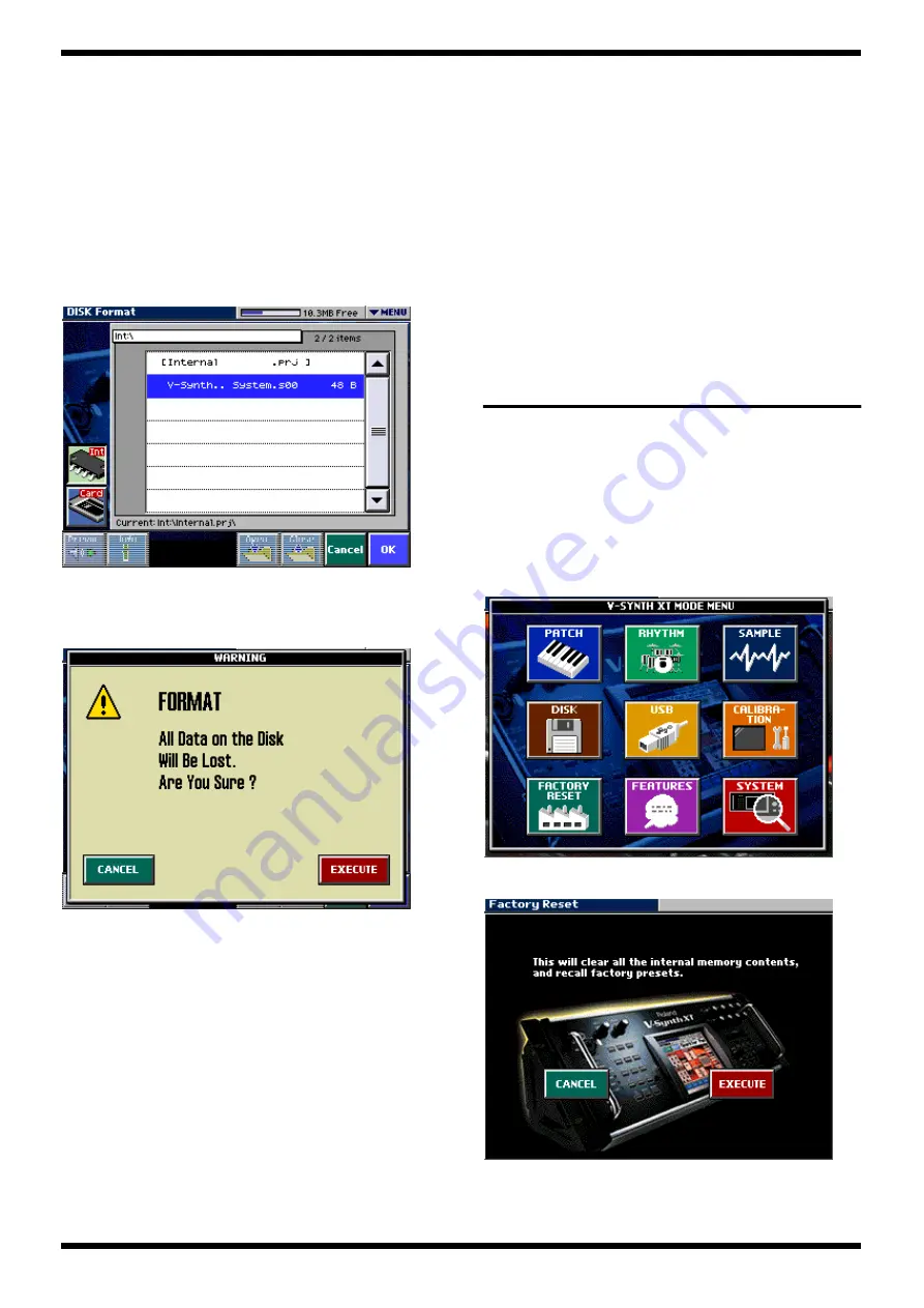
Press the <MODE> button, and touch <DISK>, <Format>.


fig.format-1.eps


2.


Touch <Int> to select the formating internal disk.


3.


Touch <OK>, then apear the warning window.

You can abort this procedure by touching <CANCEL>.


fig.format-2.eps


4.


Touch <EXECUTE> to bigin the formatting.

The all of internal disk of memory has cleard after formatting.


5.


Press <EXIT> button to back to the primaly screen.


2. Loading backup data into the V-Synth XT


The backup data is loaded into formatted disk. 


1.


Connect the V-Synth XT and PC with the USB cable according to 
“Connecting your Computer via USB (USB Mode)” (P.138) of the manual. 

Press the <MODE> button, and touch <USB>, <Internal>.

Internal disk of V-Synth XT has recognized as removable disk from PC.

The drive name is “V-SYNTH XT” on Windows XP, or “Removable Disk 
(Drive letter:)” on Windows 2000/Me.


2.


On your PC displayed copy all backup data from the drive (e.g. hard 
disk) of your PC into the “V-SYNTH XT” drive.


3.


After copying the data, operate your PC as described in “Disconnecting 
the USB connection” (p.140) of the owner’s manual, and then disconnect 
the USB cable from the V-Synth XT.


4.


Press <EXIT> button to back to the primaly screen.


3. Verifycation of the backup data.


Verifying the backup data was correctly loaded. 


1.


Press the <MODE> button, and touch <DISK>, <Tools>.

The list of the folder and the file loaded into DISK can be browse on this 
screen. 


2.


At this point, the backup data has not been loaded into the workarea of 
the V-Synth XT,

so you will be unable to check whether the process has been performed 
correctly.

Power off and turn it back on, or push the <V-CARD> button and touch 
<V-SYNTH> to reboot the system, 

you can verify the backup data is loaded correctly.


FACTORY RESET 


INSTRUCTIONS


Caution as to USER DATA


This returns all data in the V-SYNTH/XT to the factory settings (Factory 
Reset).


*

If data created by the user has already been saved in the V-Synth, all such data 
will be lost when you execute Factory Reset. Before executing Factory Reset, you 
must back up the data on your computer.


1.


Press [MODE] button. The V-SYNTH/XT MODE MENU window will 
appear.


fig.factory-1.eps


2.


Touch <FACTORY RESET>. The Factory Reset screen will appear.


fig.factory-2.eps


3.


Touch <EXECUTE> to execute Factory Reset.


4.


When Factory Reset is completed, the display will indicate “Completed”.

Содержание V-Synth XT

Страница 1: ...ODED VIEW PARTS LIST 4 15 WIRING DIAGRAM 16 PARTS LIST 18 DRIVER INSTALLATION AND SETTINGS 25 CHECKING THE VERSION NUMBER 25 USERS DATA SAVE AND LOAD 25 FACTORY RESET INSTRUCTIONS 26 UPDATING THE SYST...

Страница 2: ...rase Preset waveforms Sampling waveforms Analog Modeling 14 waves SAW SQUARE TRIANGLE SINE RAMP JUNO HQ SAW HQ SQUARE NOISE LA SAW LA SQUARE SUPER SAW FEEDBACK OSC X MOD OSC External Input Modulator 4...

Страница 3: ...Hi Z phantom power MIDI Connectors IN OUT THRU USB Connector supports USB MIDI file transfer and USB Audio Digital Audio Interface 24 bit IEC60958 COAXIAL IN OUT OPTICAL IN OUT AC Inlet Power Supply...

Страница 4: ...12D 1 11 00785856 LED SLR 342VR3F 1 12169406 LED SPACER LDS 100Y 10MM 1 12 03122112 LED BLUE SLR 343BBT3F 2 12169406 LED SPACER LDS 100Y 10MM 2 13 03120889 D S KEYTOP SX2H B GRS 5 01340290 TACT SWITC...

Страница 5: ...789 OPTICAL CONNECTOR GP1FA513TZ 1 24 03237556 OPTICAL CONNECTOR GP1FA513RZ 1 25 03231812 RCA PIN YKC21 4173 1 26 13429274 MIDI SOCKET YKF51 5041 1 27 00120434 JACK YKB21 5227 5 28 13449252 6 5MM JACK...

Страница 6: ...8 MAY 2005 EXPLODED VIEW 1 fig V SynthXT Bunkai e eps 5 4 3 1 7 6 6 2 8 1 10 11 17 16 13 14 20 9 12 15 18 19 Refer to FigA Top View1 View2 View3...

Страница 7: ...LDER AT 217K 1 6 03897534 HANDLE 2 7 03897578 PANEL PLATE 1 8 03897523 FRONT PANEL 1 9 03897545 KEY ESCT A 1 10 03897556 KEY ESCT B 1 11 72909412 LCD ASSY 1 12 72909523 PANEL KEYTOP ASSY 1 13 72909545...

Страница 8: ...ANGLE CENTER 1 22 03897612 RACK ANGLE L 1 23 03897623 RACK ANGLE R 1 24 03901634 ANGLE SPACER 2 25 03897656 SIDE COVER L 1 26 03897667 SIDE COVER R 1 27 03897490 BOTTOM CASE 1 28 72909467 JACK BOARD...

Страница 9: ...12 MAY 2005 EXPLODED VIEW 3 fig V SynthXT Heimen e eps Top View3 View1 View2 a b d c c d d d d d d e...

Страница 10: ...BZC 2 b 40011490 SCREW M3X6 PAN MACHINE W SW BZC 2 No PART CODE PART NAME DESCRIPTION Q TY c 40011478 SCREW M4X10 PAN SEMS FE ZC 4 d 40011090 SCREW 3X6 BINDING TAPTITE B BZC 4 No PART CODE PART NAME D...

Страница 11: ...14 MAY 2005 EXPLODED VIEW 4 fig V SynthXT HeimenBetsu e ep BOTTOM View4 View5 Rear Front d d d a e f a h g b d b i...

Страница 12: ...40011490 SCREW M3X6 PAN MACHINE W SW BZC 6 d 40011090 SCREW 3X6 BINDING TAPTITE B BZC 3 g 40011745 HEX NUT M4 SPRING NUT FE ZC 1 h 40011123 SCREW 4X8 BINDING TAPTITE B BZC 2 No PART CODE PART NAME DE...

Страница 13: ...PC Shield 1 0p FPC 03897934 03897890 03671856 1 0p FPC 1 0p Flex FPC Diagram Power PANEL_I O USB Analog Analog PANEL_I O X Y CFL E1 E2 E3 E4 E5 E6 E7 E8 VALUE VOLUME INPUT LCD CONT PEAK MIDI USB PHONE...

Страница 14: ...01 DISPLAY HOLDER A 1 03897512 DISPLAY HOLDER B 2 03897590 PWB HOLDER 2 01786045 SW HOLDER AT 217K 1 KNOB BUTTON 03565789 M R KNOB LF ELA BLK 1 03565234 J R KNOB SF ELA BLK SLV 10 SWITCH 01786012 SEES...

Страница 15: ...on MAB 1 03674545 K4S561632E TC75 IC SDRAM IC5 IC9 IC10 IC8 on MAB 4 02234167 AK4393 VF E2 IC DAC IC99 on MAB 1 02453878 AK4528VF IC AD DA IC98 on MAB 1 02781323 TUSB3200ACPAH IC AD DA IC69 on MAB 1...

Страница 16: ...JKB 1 15329503 DTA124EK T146 DIGITAL TRANSISTOR Q20 on JKB 1 15329533 RN2307 TE85R TRANSISTOR Q44 Q4 Q10 on JKB 3 15329521 RN1307 TE85R TRANSISTOR Q5 Q45 Q13 on JKB 3 DIODE 01780045 RB051L 40 SCHOTTK...

Страница 17: ...02 D MTL FILM RESISTOR R172 on MAB 1 03564312 RR0816P 393 D MTL FILM RESISTOR R171 on MAB 1 00566967 RPC05T 470 J MTL FILM RESISTOR R83 R126 R21 R80 R85 R84 R8 R91 R92 R12 7 R131 R86 R42 on MAB 13 005...

Страница 18: ...0J CERAMIC CAPACITOR C57 C184 C201 C63 C58 C216 C217onMAB 7 01674334 ECJ1VC1H101J CERAMIC CAPACITOR C136 C252 C212 C185 C167 C174 C204 C11 4 C165 C100 C53 on MAB C150 C151 on IVB C46 C36 on JKB C109 C...

Страница 19: ...APACITOR C103 C115 on MCB 2 02127812 RA2 25V470MT2 CHEMICAL CAPACITOR C27 C45 C164 C163 C156 C152 C178 C44 C4 1 C39 C30 C34 C25 C35 C29 on JKB C96 C180 C179 C118 C106 C99 C94 C92 C91 C89 C87 C85 C84 C...

Страница 20: ...75623 BAN CARD BNCD P 1 00 K 12 80 CN12 on JKB to CN27 on MCB 1 TRANSFORMER 03561389 EL INVERTOR DHE1105B 5VE TRANSFORMER 1 02019478 7KQ5 19832A PULSE TRANS T1 on JKB 1 SCREW 40451234 COIN SCREW M3X8...

Страница 21: ...mode will appear and the version number will be displayed in the screen fig PDTestMode00 eps Checking the version number in Patch mode 1 Touch MENU in the upper right of the screen A pulldown menu wi...

Страница 22: ...data from the drive e g hard disk of your PC into the V SYNTH XT drive 3 After copying the data operate your PC as described in Disconnecting the USB connection p 140 of the owner s manual and then di...

Страница 23: ...successful update please check the following two points Are the V Synth XT and PC correctly connected by a USB cable Were thw correct files copied to the drive that apeared on the PC desktop Please e...

Страница 24: ...peated for the test MAIN OUT PHONES Listen to the sound and verify that there is no noise or other problem with the sound Perform the impact test Lift the body of front side to a higher position about...

Страница 25: ...comes 12dB Press to proceed to the next step Verify that the waveform disappeared and OUTPUT sound muted because INPUT turns off Press to proceed to the next step Check the INPUT MIC input Connect the...

Страница 26: ...t knob all of the way to left and right and verify that the contrast changes Then adjust the knob for optimal contrast fig 13 8 eps Press A pattern in seven color stripes will appear in the LCD Verify...

Страница 27: ...eration If the check of all of the eight knobs is completed you will automatically proceed to the next test item 9 Touch Panel Calibration Calibrate the touch panel A touch pen is used for calibration...

Страница 28: ...D will be blinking for about one second and next be turned off LED of MIDI and USB turn on when all buttons of a left panel are operated Press the button of the right panel to turn off these LEDs The...

Страница 29: ...he USB cable from V Synth XT it is displayed on the screen USB Disconnect OK fig PDTestMode16 eps COMPLETE is displayed and the item of all the static test modes is completed above Turn the power off...

Страница 30: ...ID on V Synth XT was registered above 7 Press the START button on the ID Stamp dialog screen fig gidstamps eps Input the serial ID of the product seven characters to SERIAL No field of Input ID frame...

Страница 31: ...35 V SynthXT...

Страница 32: ...CARD PORT Bus Knobs Storage Photo x4 DECODER CODEC 44 1K 48K 96K OPT OUT BOARD Output IC7 Bus TUSB System 1 2 IC10 IC1 SW JK5 DSP SSOC SUPPLY Regulator L18 ESP4 8 DRAM TUSB3200 16 FLASH I F 5 7 32 COA...

Страница 33: ...38 MAY 2005 CIRCUIT BOARD MAIN fig b main1 eps View from components side...

Страница 34: ...39 V SynthXT CIRCUIT BOARD MAIN fig b main2 eps View from foil side...

Страница 35: ...34 RA30 C84 C15 R48 R49 R47 C85 RA44 C80 RA13 R82 R35 R19 R59 C48 R37 RA26 C69 RA38 RA14 RA7 IC8 R40 R68 R62 IC10 RA2 C78 R81 RA43 R80 IC1 C47 C17 C16 C42 RA3 R39 RA8 R88 R86 R87 C76 C77 IC1 C2 RA6 C6...

Страница 36: ...L8 C103 C126 R132 R110 IC35 C104 C116 IC41 C152 C97 C127 C145 RA46 R101 C98 RA45 L15 R137 C107 R123 R134 R109 IC30 IC30 C143 C113 C144 L14 R116 L13 R117 C119 C109 R108 C110 R118 RA53 R115 R135 IC36 C1...

Страница 37: ...44 RA67 C170 C171 Q4 IC52 IC52 IC57 Q3 C158 C174 C167 C160 R146 R125 IC51 IC53 IC53 L17 R149 IC56 R150 IC57 C168 R143 C166 IC57 R141 IC51 R140 R138 RA62 C159 IC51 IC57 IC49 RA63 C173 IC48 IC51 R151 Q5...

Страница 38: ...67 C194 L18 D3 R196 C217 R182 R181 R178 C212 C181 C180 R167 IC68 R210 C209 D2 IC71 RA72 C201 R206 R211 R161 IC84 R193 C205 R198 R204 R189 IC71 R203 C175 R205 R154 R166 X2 R163 C216 LED3 CN6 C189 R184...

Страница 39: ...R238 C242 C233 C252 R226 D7 C228 IC99 R232 R231 C250 R236 IC105 RA74 C240 IC105 R225 C238 R243 R228 L22 C254 L24 L23 IC97 C236 C235 IC100 R234 IC95 X3 C239 R244 R245 IC105 C227 IC100 C251 R230 IC97 IC...

Страница 40: ...51 MAY 2005 V SynthXT CIRCUIT BOARD PANEL fig b panel1 eps View from components side...

Страница 41: ...53 MAY 2005 V SynthXT CIRCUIT BOARD PANEL fig b panel2 eps View from foil side...

Страница 42: ...VR11B EVUF2A 10 20 VR11A EVUF2A 1 2 3 LED5 SLR 343DUT32 1 2 DA2 MA142WK TX 1 2 3 DA3 MA142WK TX 1 2 3 DA4 MA142WK TX 1 2 3 DA5 MA142WK TX 1 2 3 DA6 MA142WK TX 1 2 3 DA7 MA142WK TX 1 2 3 C10 NIU C9 NI...

Страница 43: ...EVQ11A05R 1 2 SW20 EVQ11A05R 1 2 SW18 EVQ11A05R 1 2 SW19 EVQ11A05R 1 2 DA11 MA142WK TX 1 2 3 SW16 EVQ11A05R 1 2 EN1A EVQB1SA EN A B 3 2 1 4 5 CN3 10FMN BTK A 1 1 2 2 3 3 4 4 5 5 6 6 7 7 8 8 9 9 10 10...

Страница 44: ...57 V SynthXT CIRCUIT DIAGRAM INLET 1 1 fig c inlet eps INLET BOARD JK1 PWI 1818 FANTOM WIRING W3 2 1 CN6 2P3 SDN V SYNTH XT WIRING W1 1 1 3 3...

Страница 45: ...59 MAY 2005 V SynthXT CIRCUIT BOARD JACK fig b jack1 eps View from components side...

Страница 46: ...61 MAY 2005 V SynthXT CIRCUIT BOARD JACK fig b jack2 eps View from foil side...

Страница 47: ...P IC5C M5218AFP 8 4 C48 0 1 C44 RA2 V M 47 25 R12 RR0816 D 3 3K R53 RPC05T J 1K R8 RR1220P D 330 R15 RR1220P D 10K R30 RR1220P D 10K R48 RR0816 D 330 R26 RR0816 D 3 3K R7 RR0816 D 680 R196 RR1220P D 1...

Страница 48: ...FT 13 12 FG T1 7KQ5 3 1 6 4 2 10 20 C64 10P C65 10P JK9B YKC21 4173 22 21 L14 N1608Z T01 C62 0 01 ECJ1VB1H DA12 MA142WK TX 1 2 3 C71 0 1 R96 RPC05T J 10K IN 2 4 5 2 5 4 4 2 5 OUT THRU JK8 YKF51 5041 1...

Страница 49: ...2 3 4 5 6 7 8 1 2 3 4 5 6 7 8 C95 0 1 C104 ECJ1VC1H 100P C110 ECJ1V 33P C98 0 1 JK12 YKF45 0021 1 2 3 4 10 20 L18 EXCML16A IC13B NE5532AP 6 5 7 C165 ECJ1V 33P R108 RPC50T J 47 1 2W R123 RPC05T J 100K...

Страница 50: ...A21 IOB2 T7 PA7 A20 VCC T8 B0 CS7 MO0 T9 B1 CS6 MIO1 T10 B2 CS5 MO2 T11 B3 CS4 MIO3 T12 B4 T13 B5 T14 B6 T15 B7 RESO FWE VSS TXD0 P90 TXD1 P91 RXD0 P92 RXD1 P93 IRQ4 SCK0 P94 IRQ5 SCK1 P95 P40 D0 P41...

Страница 51: ...3 34 35 36 37 38 39 40 41 42 43 44 45 46 47 48 49 50 51 52 53 54 55 56 57 58 59 60 61 62 63 64 65 66 67 68 GND D3 D4 D5 D6 D7 CE1 A10 OE A11 A9 A8 A13 A14 WE PGM RDY BSY VCC VPP A16 A15 A12 A7 A6 A5 A...

Страница 52: ...ly individually import the patches or sam ples that you want to use DISK Path Duplicate You are attempting to write to the same hierarchical level Change the writing destination DISK Path Name Too Lon...

Страница 53: ...D DEMO Replace All Data Are You Sure When you load the demo data all data in the VP 9000 will be lost Is it OK to execute the operation To cancel the operation touch CANCEL If you wish to load the dem...

Страница 54: ...name before you execute p 137 MIDI Buffer Full An excessive amount of MIDI data was received all at once and could not be processed properly MIDI Communication Error A MIDI hardware error has occurred...

Отзывы: