


EFR32BG22
Shenzhen RF-star Technology Co., Ltd.
Page 82 of 93
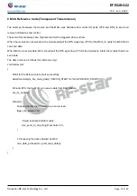
9.2.3 External Antenna Design Recommendation of the Half-Hole ANT Pin
1.
A Π-type matching circuit is reserved for the antenna, and 50 Ω impedance control is performed on the RF traces.
The traces are as short as possible, and 135° or arc traces are used as much as possible. No vias are used to
change layers. More GND vias are placed around the RF traces.
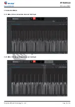
Figure 14. Reference Design of the External Antenna
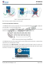
Figure 15. Reference Design of the External Antenna Traces
2.
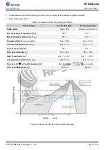
The RF trace width and copper-clad spacing can be calculated by SI9000 software, and the impedance is controlled
to 50 Ω according to the actual board thickness, number of layers, plate, dielectric thickness, dielectric constant,
copper thickness, line width, line spacing, and solder mask thickness.
Example: FR4 is a double-layer board with a thickness of 1.0 mm. Through calculation, the width of the trace is
0.8254 mm, and the spacing between traces and copper is 0.22 mm.
Figure 16. SI9000 Impedance Calculation Diagram
Содержание EFR32BG22
Страница 71: ...EFR32BG22 www szrfstar com V1 6 Jun 2022 Shenzhen RF star Technology Co Ltd Page 70 of 93...
Страница 75: ...EFR32BG22 www szrfstar com V1 6 Jun 2022 Shenzhen RF star Technology Co Ltd Page 74 of 93...
Страница 76: ...EFR32BG22 www szrfstar com V1 6 Jun 2022 Shenzhen RF star Technology Co Ltd Page 75 of 93...
Страница 77: ...EFR32BG22 www szrfstar com V1 6 Jun 2022 Shenzhen RF star Technology Co Ltd Page 76 of 93...
Страница 91: ...EFR32BG22 www szrfstar com V1 6 Jun 2022 Shenzhen RF star Technology Co Ltd Page 90 of 93 CE...