


Hardware Design Specification
ASD-B-16-0247 Rev1.3
Page 44 of 105
September 8, 2017
RTK00V2XRC7746SFS
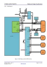
3.16
Connection between CPU and MCU
3.16.1
Specifications
The Tethys board have a MCU to control the Power sequence and Reset sequence. The power sequence and reset sequence are shown
as Figure 23 and Figure 21 respectively in the next chapter.
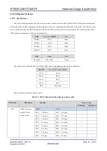
The Tethys and MCU connection include MSIOF0 and I2C1 and RESET signal. The corresponding signals are shown as below:
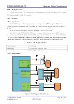
HSCIF2 connection:
R-Car-W2H
Signal
MCU signal
MSIOF0_RXD_A
P11_9/CSIG1SO/RLIN35RX/INTP15/PWGA49O/TAUB1I13/TAUB1O13/MEMC0CS1
MSIOF0_SCK_A
P11_10/CSIG1SC/PWGA50O/TAUB1I15/TAUB1O15/MEMC0CS2/ETNB0COL
MSIOF0_TXD_A
P11_11/CSIG1SI/RLIN25TX/PWGA51O/TAUB1I0/TAUB1O0/MEMC0CS3/ETNB0RXDV
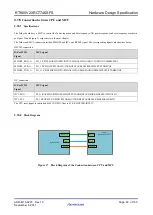
I2C connection:
R-Car-W2H
Signal
MCU signal
I2C1-SDA
P0_11/RIIC0SDA/DPIN12/CSIH1CSS2/TAUB0I8/TAUB0O8/RLIN26RX/PWGA34O
I2C1-SCL
P0_12/RIIC0SCL/DPIN13/PWGA45O/TAUB0I10/TAUB0O10/CSIG0SI/RLIN26TX
The CPU reset signal is controlled by MCU GPIO. That is P1_0/RLIN33RX/INTP13.
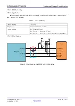
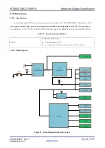
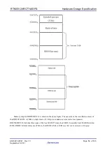
3.16.2
Block Diagram
Rcar-W2H
MSIOF
I2C1
RESET
MSIOF1_B
I2C1
RESET
MCU
RH850F1H/F1L
RIIC0
RESET
RLIN
Figure 17 Block Diagram of the Connection between CPU and MCU


