Hardware Design Specification
ASD-B-16-0247 Rev1.3
Page 69 of 105
September 8, 2017
RTK00V2XRC7746SFS
6.3
The details of connectors
(1)
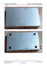
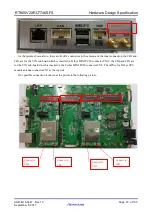
There are two USB connectors, the CN1B is corresponding to Tethys from HUB and CN1A is
corresponding to Tethys from W2H respectively as the picture shown above.
(2)
The CAN pin assignments are shown as below:
CN6 PIN Number
Signal
Remark
1
CPU_CAN0_H
HIGH-level CAN bus line
2
CPU_CAN0_L
LOW-level CAN bus line
3
MCU_CAN0_H
HIGH-level CAN bus line
4
MCU_CAN0_L
LOW-level CAN bus line
5
MCU_CAN1_H
HIGH-level CAN bus line
6
MCU_CAN1_L
LOW-level CAN bus line
7
BP
Flexray bus line plus
8
BM
Flexray bus line minus
9
GND
Ground
10
GND
Ground
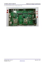
As the picture shown above, there are there USB2UART connectors from the left to right as the figure
shown, they are for MCU debug, sub board V2X debug and CPU debug respectively.
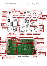
MCU Debug
CPU Debug
Sub Board V2X
Debug
CH2 & CH3 GPS:
to V2X SUB(CN12) to Tethys CN7
2 4 6 8 10
1 3 5 7 9
CN1B: USB1
CN1A:USB0

