background image


Hardware Design Specification 

ASD-B-16-0247    Rev1.3 


Page  59  of 105 

September 8, 2017 


RTK00V2XRC7746SFS 

4.2.3 

Realize an asynchronous serial with baud rate of 1M between RH850 and CPU. 

This UART uses RLIN30 of RH850’s LIN/UART interface. The operations are same as above. 

4.2.4 

Make CAN0 and CAN1 working with baud rate of 1M 

1.


CAN0 sends 4-byte data only once. 

2.


CAN1 receives the data coming from CAN0. 

3.


Once CAN1 receives, the wave form can not be monitored. 

The flow chart is as follows 


YES 

END 

NO 

START 

Initialize can0 

    and can1 

Can0 sends 

4-byte data 

Can1 has received 

            the data 

Содержание RTK00V2XRC7746SFS

Страница 1: ...ons represents information on the product at the time of publication and is subject to change by Renesas Electronics Corp without notice Please review the latest information published by Renesas Electronics Corp RTK00V2XRC7746SFS User s Manual Hardware Rev 1 3 September 2017 ASD B 16 0247 ...

Страница 2: ...f Boot Device 15 3 1 4 MD4 Pin Selection of CS0 Space Size 15 3 1 5 MD5 Pin Reserved 15 3 1 6 MD 7 6 Pins Selection of Master Boot Processor 15 3 1 7 MD8 Pin Selection of Area 0 Space Data Bus Width 16 3 1 8 MD9 Pin Selection of Crystal Resonator or Crystal Oscillator 16 3 1 9 MD21 MD20 MD11 MD10 and MDT 1 0 Pins Switching of JTAG SDHI1 and SDHI2 16 3 1 10 MD 14 13 Pins Frequency Mode Setting 17 3...

Страница 3: ... 31 3 10 DEBUG INTERFACE 32 3 10 1 CPU debug 32 3 10 2 CPU JTAG2 debug 33 3 10 3 MCU debug 34 3 11 GYRO G SENSOR 35 3 11 1 Specifications 35 3 11 2 Block Diagram 35 3 12 I2C INTERFACES 36 3 12 1 Specifications 36 3 12 2 List of Slave Addresses 37 3 12 3 Block Diagram 37 3 13 GPS MODULE 38 3 13 1 Specifications 38 3 13 2 Block Diagram 38 3 14 CAN AND FLEXRAY INTERFACE 39 3 14 1 Specifications 39 3 ...

Страница 4: ...3 4 2 FUNCTION 57 4 2 1 Control the power of the Tethys Custom Board 57 4 2 2 Realize the UART with the baud rate of 115200 58 4 2 3 Realize an asynchronous serial with baud rate of 1M between RH850 and CPU 59 4 2 4 Make CAN0 and CAN1 working with baud rate of 1M 59 5 OUTLINE DIAGRAMS OF THE TETHYS BOARD 60 5 1 TETHYS BOARD DIMENSION 60 5 2 THE WEIGHT OF THE TETHYS BOARD 60 5 3 TETHYS ID DIMENSION...

Страница 5: ... 1 Specifications 92 7 7 2 Block Structure 92 7 7 3 Block Diagram 93 7 8 V2X CONNECTION BOARD 94 7 8 1 Board Structure 94 7 8 2 Block Diagram 95 7 8 3 Block dimension 95 7 9 SUB BOARD TORTUGA WIRELESS MODULE BOARD DIMENSION 96 7 9 1 RF characteristic 96 7 9 2 Board Dimension 98 7 10 SIDE COVER OPTION OF CASE 100 7 11 ACRONYMS AND ABBREVIATIONS 101 8 REGULATORY WARNING STATEMENTS 102 9 EU DECLARATI...

Страница 6: ...cification 34 Table 15 GYRO G SENSOR Specifications 35 Table 16 List of I2C Devices 36 Table 17 List of I2C Slave Addresses 37 Table 18 CAN and Flexray Interface Specifications 39 Table 19 DIP Switches default setting is as below table 41 Table 20 Slide Switches default setting is as below table 43 Table 21 List of Clock Signals and Crystals for the R Car W2H 45 Table 22 List of Differential Clock...

Страница 7: ...gure 16 Block Diagram of the CAN and Flexray Interface 39 Figure 17 Block Diagram of the Connection between CPU and MCU 44 Figure 18 Block Diagram of the Clock system 46 Figure 19 Block Diagram of the External Interrupts 47 Figure 20 Block Diagram of the Reset System 48 Figure 21 The Reset Sequence 49 Figure 22 Block Diagram of the Power System 51 Figure 23 The Power Sequence 52 Figure 24 The Teth...

Страница 8: ...tenna2 SMA rotate 90 degree 90 Figure 45 Image of V2X Antenna2 SMA rotate 0 degree 90 Figure 46 RF Cable 91 Figure 47 JTAG Debug Board with FPC Cable for R CAR W2H RH850 MCU 92 Figure 48 JTAG Debug Board block structure 92 Figure 49 Block Diagram of the JTAG Debug Board 93 Figure 50 Top side view of V2X Connection board 94 Figure 51 Bottom side view of V2X Connection board 94 Figure 52 Block struc...

Страница 9: ...s board allows developers to efficiently conduct required tasks such as evaluating the performance of R Car W2H based systems thus greatly reducing turn around times in product development SD Card CN2 GPS Antenna CN7 HSM CN14 CAN Flexray CN6 Ethernet CN3 Audio jack J1 USB CN1 DEBUG CN4 POWER Switch SW18 POWER IN JACK CN17 and CN18 Micro USB CN16 CN10 CN5 ETNB CN13 D12 GPS_LED D4 D6 D8 D10 CN9 CN8 ...

Страница 10: ...are not support CN7 GPS ANT Connector CN14 HSM Connector Software not support CN13 ETNB Connector Software not support PCIE Connectors CN9 Mini PCIE Connector for V2X Sub Board CN8 Mini PCIE Connector for Ethernet AVB Sub Board Software not support CN12 Mini PCIE Connector for V2X Sub Board CN11 Standard Mini PCIE Debugger Interfaces CN4 26 pin FPC connector for CPU and MCU CN10 UART USB for Debug...

Страница 11: ...dule ROM QSPI QSPI0 SPI Flash 64MB QSPI1 SPI Flash 4MB Ethernet MAC Ethernet AVB Ethernet MAC RJ45 Connector Ethernet AVB Mini PCIE Connector for Ethernet AVB Sub Board Ethernet AVB s software not support HSCIF HSCIF1_A Mini PCIE Connector for Ethernet AVB Sub Board Ethernet AVB s software not support SCIF0_D HSCIF0_B 1 Mini PCIE Connector for V2X Sub Board 2 UART USB SCIF3_B HSCIF2 Mini PCIE Conn...

Страница 12: ... Be sure to confirm that the ACC switch SW18 is off before plugging the AC adapter into the power source It is prohibited to plug the AC adapter into a power source while the ACC switch SW18 is on 2 When turning off the power Be sure to turn off the ACC switch SW18 before unplugging the AC adapter from the power source It is prohibited to unplug the AC adapter from the power source while the ACC s...

Страница 13: ... FH12 20S 0 5SV Irios GPS Module NEO 7M U blox GPS ANT U FL R SMT Murata CAN CN TSW 104 08 F D Samtec RMII PHY KSZ8041RNLI Micrel SPI Flash 4MB S25FL132K0XMFI011 Spansion SPI Flash 64MB S25FL512SAGMFIG11 Spansion GPIO GPIO CPU R CarW2H Renesas BU12V CAN transceiver TJA1050 NXP CAN transceiver TJA1050 NXP Mini PCI Express CN 1759546 1 TE Mini PCI Express CN 1759546 1 TE USB micro B CN 47346 0001 Mo...

Страница 14: ...A Operating Temperature 25 25 85 Degree C V2X antenna Frequency range 5860 5920 MHz V2X antenna VSWR 2 0 V2X antenna Gain 2M Cable Type 1 3 0 without cable loss 2 1 0 with cable loss Rod Type 1 5 0 dBi V2X antenna Cable Loss 4 0 L 2m dB GPS antenna Center Frequency 1575 3 MHz GPS antenna VSWR 2 0 GPS antenna Bandwidth 20 MHz GPS antenna Gain 30 dB Storage Temperature 25 85 Degree C Operating Humid...

Страница 15: ...3 MD 3 1 Pins Selection of Boot Device These pins select the boot device MD3 MD2 MD1 Selection of Boot Device 0 0 0 External ROM boot area 0 0 0 1 eMMC boot via SDHI1 0 1 0 Serial flash ROM boot via QSPI 16Kbytes transferred at 48 75 MHz 0 1 1 Reserved 1 0 0 Serial flash ROM boot via QSPI 16Kbytes transferred at 39 MHz 1 0 1 Reserved 1 1 0 Serial flash ROM boot via QSPI 4 Kbytes transferred at 39 ...

Страница 16: ...al clock is input to the EXTAL pin 1 A crystal resonator is connected to the EXTAL and XTAL pins 3 1 9 MD21 MD20 MD11 MD10 and MDT 1 0 Pins Switching of JTAG SDHI1 and SDHI2 These pins select the debugging function through the JTAG connector CN4 or the SD card slot for the SDHI1 The debugging through the SDHI1 or SDHI2 is possible by the combination of MD pin settings in the R Car W2H specificatio...

Страница 17: ...3 1 11 Initial Values of Mode Setting Pins on Tethys Board The following table shows the Initial Values of Mode Setting Pins on the Board and how the individual mode pins are set MD Pins Initial Value Initial Function Setting Method MD0 0 Set by a dip switch MD 3 1 010 Boot from the QSPI 48 75 MHz 16 Kbyte transfer Set by a dip switch MD4 0 CS0 space size 64 Mbytes Set by a dip switch MD5 1 Set by...

Страница 18: ... for DDR3 SDRAM DBSC in the R Car W2H Product name MT41K256M16HA 125 AAT E from Micron DDR3 1600 x 16 bits 4 Gbits x 2 pcs Power supply voltage 1 50 V Capacity H 01_0000 0000 to H 01_FFFF FFFF Bus width 32 bit data bus Memory bus frequency R Car W2H Spec DDR3 1000 3 2 2 Signal Connections between R Car W2H and DDR3 SDRAMs Table 5 Signal Connections between R Car W2H and DDR3 SDRAMs R Car W2H DDR3 ...

Страница 19: ...0CKE1 M0ODT1 M0CK1 M0CK1 M0DQS 3 2 M0DQS 3 2 M0DM 3 2 M0BKPRST M0VREFDQ1 M0VREFDQ0 M0VREFCA M0ZQ A 15 0 BA 2 0 RAS CAS WE RESET CS CKE ODT CK CK DQS DQS DM DQS DQS DM DQL 7 0 DQU 7 0 VREFCA VREFDQ DQL 7 0 DQU 7 0 0 1uF 0 1uF 0 1uF 20K 20K DDR3 0 1uF 0 1uF 0 1uF 20K 20K M0BKPRST D1 5V D1 5V 120 MT41K256M16H A 125 AAT E 0 1uF 0 1uF 20K 20K 22 22 22 22 22 M0CS1 CS 22 22 CKE 22 22 22 100 M0ZQ 240 ODT ...

Страница 20: ...tions Flash memory interfaces QSPI0 and QSPI1 in the R Car W2H Operating voltage D3 3 V_FLASH 3 3V Capacity 512 Mbit and 32 Mbit Mapping area 512 Mbit 0x0000000 0x3ffffff Mapping area 32 Mbit 0x0000000 0x3fffff 3 3 2 Block Diagram R Car W2H SPI FLASH S25FL132K0XMFI011 32Mbit U6 GP1_21 QSPI0_SSL WE1 GP1_20 QSPI0_IO3 RD GP1_19 QSPI0_IO2 CS0 GP1_18 QSPI0_MISO QSPI0_IO1 RD WR GP1_17 QSPI0_MOSI QSPI0_I...

Страница 21: ...ifications Controller On chip SSI0and SSI1 in the R Car W2H Audio codec AK4642EN U29 from AKM I2C bus Interface 1 I2C slave address 0x25 for read 0x24 for write CAD0 0 Master slave mode AK4642EN Master slave selectable slave mode by default Audio connector MIC IN J1 LINE OUT J1 3 4 2 Block Diagram U1 R Car W2H GP5_9 SSI_SCK0129_A GP5_10 SSI_WS0129_A U29 AUDIO AK4642EN GP5_11 SSI_SDATA0_A LRCK BICK...

Страница 22: ... chip MMC interface of the R Car W2H For details on the MMC see the R Car W2H Hardware Manual Table 8 eMMC Memory Interface eMMC Specifications MMC controller On chip MMC in the R Car W2H Interface voltage control D3 3V_eMMC 3 3V eMMC memory SDIN8DE1 8G XA U7 from SanDisk Capacity 8GB 3 5 2 Block Diagram MMC_CLK MMC_CMD MMC_D 7 0 VCCQ_MMC eMMC CLK CMD DATA 7 0 D3 3V VCCQ VCC D3 3V_eMMC 10K D3 3V_e...

Страница 23: ... please refer to the R Car W2H hardware manual CN12 and CN2 can not be used at the same time Table 9 Specifications of SD Card Host Interface SDHI2 SD Host Interface On chip SDHI2 in the R Car W2H Voltage control for VDD VCCQ_SD2 3 3V 1 8V it can be switched by software D3 3V 3 3V SD Card Slot 503182 1852 CN2 from Molex 3 6 2 Block Diagram R Car W2H SDHI2 SD2_CLK SD2_DATA 3 0 SD2_CD SD2_WP SD2_CMD...

Страница 24: ... are shown as below 3 7 2 1 CN9 of figure 7 signal assignments are shown as below Pin NO Signal I O Remark Pin NO Signal I O Remark 1 C2X0_DCMODE O GPIO 2 D3 3V PO Power 3 N C 4 GND Power 5 PCIE_5 0V PO Power 6 PCIE_5 0V PO Power 7 C2X0_RESETB O GPIO 8 GPS_1PPS C2X0_GPIO_B3 I O GPS 1PPS output or GPIO 9 GND Power 10 C2X0_GPIO_B2 I O GPIO 11 RX0_D C2X_RXD I UART from CPU or USB2UART 12 C2X0_GPIO_B1...

Страница 25: ...2 C2X1_GPIO_B1 I O GPIO 13 TX3_B O UART from CPU 14 C2X1_GPIO_B0 I O GPIO 15 GND Power 16 C2X1_STATE I C2X state 17 N C 18 GND Power 19 N C 20 C2X1_GPIO_A6 I O GPIO 21 GND Power 22 C2X1_GPIO_A5 I O GPIO 23 HRX2 I UART from CPU 24 PCIE_5 0V PO Power 25 HTX2 O UART from CPU 26 GND Power 27 GND Power 28 PCIE_5 0V PO Power 29 GND Power 30 C2X1_GPIO_A4 I O GPIO 31 HCTS2 I O UART from CPU 32 C2X1_GPIO_A...

Страница 26: ...r 16 ETH_MDIO AVB_RXD2 I Receive data signal 17 AVB_TX_CLK I Transmit clock signal 18 GND Power 19 C2X1_RESETB AVB_GTX_CLK O GMII transmit clock signal 20 ETH_REF_CLK AVB_RX_CLK I Receive clock signal 21 GND Power 22 AVB_RESETn O GPIO 23 HRX1_A I High speed uart 24 PCIE_5 0V PO Power 25 HTX1_A O High speed uart 26 GND Power 27 C2X1_GPIO_A1 AVB_TXD7 O Transmit data signal 28 PCIE_5 0V PO Power 29 C...

Страница 27: ...wer 3 N C 4 GND Power 5 N C 6 D1 5V PO Power 7 N C 8 N C 9 GND Power 10 N C 11 PCIe_CLKN I PCIe clock minus 12 N C 13 PCIe_CLKP I PCIe clock plus 14 N C 15 GND Power 16 N C 17 N C 18 GND Power 19 N C 20 N C 21 GND Power 22 N C 23 PCIe_RXN I PCIe receive data minus 24 D3 3V PO Power 25 PCIe_RXP I PCIe receive data plus 26 GND Power 27 GND Power 28 D1 5V PO Power 29 GND Power 30 I2C1 SCL I O I2C clo...

Страница 28: ...N C 52 D3 3V PO Power 3 7 3 Block Diagram R car W2H SDHI0 Mini PCI Express CN TE CN9 GPIO SCIF0 HSCIF0 SDHI2 Mini PCI Express CN TE CN12 GPIO Mini PCI Express CN TE CN8 1PPS USB 2 0 1PPS SCIF3 HSCIF2 EtherAVB GPIO USB 2 0 HSCIF1 Mini PCI Express CN TE CN11 PCIe USB 2 0 I2C Figure 7 Block Diagram of Mini PCI Express Interface ...

Страница 29: ...ons USB to UART IC CP2102 GM from Silicon USB function connector 47346 0001 from Molex x 3pcs Common mode filter with ESD protection diode PRTR5V0U2X from NXP x 3pcs 3 8 2 Block Diagram R car W2H MCU USB to UART CP2102 Silicon USB micro B CN CN10 USB to UART CP2102 Silicon USB micro B CN CN5 SCIF2 debug USB to UART CP2102 Silicon USB micro B CN CN16 Mini PCI Express CN TE ESD protection PRTR5V0U2X...

Страница 30: ...Genesys to expand 4 USB 2 0 The expand 1 port of the GL852GT is connected to a USB 2 0 type A port There is a switch IC for the two USB ports power supply The other 3 USB port of the GL650USB are connected to the three of four mini PCIE connectors separately Table 11 USB2 0 Interface USB controller On chip USB2 0 function controller in the R Car W2H USB Power Switch BD2066FJ LBE2 from ROHM USB Hub...

Страница 31: ...VC USB0_PWEN USB0_OVC 10K USB 2 0 BD2066FJ LBE2 0 0 Mini PCI Express CN TE CN8 USB 2 0 H type A CN 2 in1 1775468 1 TE CN1 Mini PCI Express CN TE CN12 Mini PCI Express CN TE CN11 DP0 DM0 DP1 DM1 DP2 DM2 DP3 DM3 DP4 DM4 OVCUR1 PWRENB1 OVCUR1 PWRENB1 OVCUR1 PWRENB1 OVCUR1 PWRENB1 GL852GT R car W2H RESET 12M D3 3V 10K D3 3V 10K 10K D3 3V PWRENB1 OVCUR1 OVCUR1 PWRENB1 1K SYS_RESETn_33 ESD Protection PR...

Страница 32: ...nnecting the USB B connector to the host PC through a USB cable The SCIF2 of the R Car W2H is connected to the USB B connector via the USB to UART Bridge CP2102 The R Car W2H incorporates the Ethernet MAC that supports 100Base T or 10Base T compliant with IEEE 802 3u On the Tethys board the Ethernet MAC signals are connected to the RMII PHY interface KSZ8041RNLI manufactured by Micrel Table 12 CPU...

Страница 33: ...bug Interface CN4 IMSA 9632S 26Y801 from IRISO operating conditions The SW12 switch 2 1 short The SW1 switch 9 8 short switch 10 7 short The SW2 switch 8 1 short switch 7 2 short switch 6 3 short switch 5 4 short 3 10 2 2 Block Diagram D1 8V 10K R Car W2H U1 JTAG CN CN4 D1 8V 10K 10K SW12 3 1 2 MMC0_CMD_TRST MMC0_D2_TDI MMC0_D1_TMS MMC0_D0_TCK MMC0_D3_ASEBRK ACK MMC0_CLK_TDO 5 4 3 6 7 2 8 1 SW2 9 ...

Страница 34: ...o test the connection between the devices mounted on the printed circuit board The SW17 switch 2 3 short is for normal operation and 2 1 short for MCU Debug Table 14 MCU debug Specification Control Interface MCU Debug Debug Interface CN4 IMSA 9632S 26Y801 from IRISO operating conditions The SW17 switch 2 1 short for MCU Debug 3 10 3 2 Block Diagram DCUTCK DCUTMS DCUTRST BU3 3V DCUTDO DCUTDI 4 7K R...

Страница 35: ...e The AIS328DQ is an ultra low power high performance 3 axis linear accelerometer The CPU communicates with the A3G4250D and AIS328DQ through its I2C1 and GPIOs Table 15 GYRO G SENSOR Specifications Controller R Car W2H Control Interface The A3G4250D and AIS328DQ from ST Supply voltage D3 3V 3 3V 3 11 2 Block Diagram SDO SA0 CS SCL SDA DRDY INT2 INT1 SDO SA0 CS SCL SDA INT1 INT2 D3 3V SCL1 SDA1 GP...

Страница 36: ...erfaces 1 In order to compensate for the driving ability of the R Car W2H the Tethys board incorporates an LTC4313IMS8 1 PBF I2C buffer manufactured by Linear Technology through which each I2C device is connected to the I2C interface for the device The following devices are connected to each I2C interface on the Tethys board Table 16 List of I2C Devices I2C Controller On chip I2C controllers in th...

Страница 37: ...0D GYRO 1 1 0 1 0 1 1 x 0xD7 0xD6 2 U29 AK4642EN AUDIO 0 0 1 0 0 1 0 x 0x25 0x24 3 U30 AIS328DQ G SENSOR 0 0 1 1 0 0 1 x 0x33 0x32 4 U32 RH850F1H F1L MCU 5 CN11 Mini PCIE Connector CN14 HSM CN Connector Note 1 Pins 3 to 1 A 2 0 GND 2 Pin 8 to 12 RESERVED 5 1 GND 3 Pin 8 CSN CAD0 GND 4 Pin 25 EP and Pin 4 RESERVED1 GND 5 I2C no use 3 12 3 Block Diagram U2 LTC4313IMS8 1 PBF U1 R CarW2H SCL1_A SDA1_A...

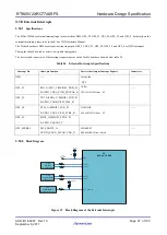
Страница 38: ...ications The NEO 7P 7M M8L manufactured by UBLOX is a high performance GPS module It has high performance active antenna It communicates with the CPU through the SCIF5 interface 3 13 2 Block Diagram GPS Receiver Module NEO 7P 7M M8L TXD RXD SCIF5 R Car W2H CN7 U FL R SMT Hirose GPS Antenna Figure 15 Block Diagram of the GPS module ...

Страница 39: ...exray driver TJA1082 manufactured by NXP is used for the Flexray bus Table 18 CAN and Flexray Interface Specifications Controller R Car W2H and RH850F1H F1L if mounting RH850F1L not Flexray function Control Interface CN6 HTST 105 04 S D RA from Samtec CAN Transceiver Interface TJA1050 from NXP Flexray Transceiver Interface TJA1082 from NXP 3 14 2 Block Diagram CAN transceiver TJA1050 NXP U19 R car...

Страница 40: ... shown as below CN6 PIN Number Signal Remark 1 CPU_CAN0_H HIGH level CAN bus line 2 CPU_CAN0_L LOW level CAN bus line 3 MCU_CAN0_H HIGH level CAN bus line 4 MCU_CAN0_L LOW level CAN bus line 5 MCU_CAN1_H HIGH level CAN bus line 6 MCU_CAN1_L LOW level CAN bus line 7 BP Flexray bus line plus 8 BM Flexray bus line minus 9 GND Ground 10 GND Ground ...

Страница 41: ...ED R Car W2H PORT Color D3 D4 GP5_4 Green D5 D6 GP5_5 Green D7 D8 GP5_6 Green D9 D10 GP5_7 Green LED Signal Color D11 D12 GPS_1PPS Green The tactile switch controlled by R Car W2H or MCU port correspondingly is shown as the table below Tact SW R Car W2H or MCU PORT SW13 GP5_0 SW14 GP5_1 SW15 GP5_2 SW16 GP5_3 SW4 MCU reset There are other Switches are listed as below Table 19 DIP Switches default s...

Страница 42: ...ort SW6 1 16 open MD9 SW6 2 15 short SW6 2 15 open MD10 SW6 3 14 short SW6 3 14 open MD11 SW6 4 13 short SW6 4 13 open MD13 SW6 5 12 short SW6 5 12 open MD14 SW6 6 11 short SW6 6 11 open MD20 SW6 7 10 short SW6 7 10 open MD21 SW6 8 9 short SW6 8 9 open SW7 Mode select switch Mode 0 Mode 1 MDT0 SW7 1 4 short SW7 1 4 open MDT1 SW7 2 3 short SW7 2 3 open SW8 Ethernet MAC and Ethernet AVB Selected swi...

Страница 43: ... SW11 1 4 short SW11 2 3 open SW11 2 3 short Table 20 Slide Switches default setting is as below table Slide Switch Description Function Default setting ON Short OFF Open SW3 JTAG Debug Normal Operation select switch JTAG Debug Normal operation SW3 1 2 short SW3 1 2 open SW3 2 3 open SW3 2 3 short SW12 JTAG Debug Normal Operation select switch JTAG2 Debug Normal operation SW12 1 2 short SW12 1 2 o...

Страница 44: ...r W2H Signal MCU signal MSIOF0_RXD_A P11_9 CSIG1SO RLIN35RX INTP15 PWGA49O TAUB1I13 TAUB1O13 MEMC0CS1 MSIOF0_SCK_A P11_10 CSIG1SC PWGA50O TAUB1I15 TAUB1O15 MEMC0CS2 ETNB0COL MSIOF0_TXD_A P11_11 CSIG1SI RLIN25TX PWGA51O TAUB1I0 TAUB1O0 MEMC0CS3 ETNB0RXDV I2C connection R Car W2H Signal MCU signal I2C1 SDA P0_11 RIIC0SDA DPIN12 CSIH1CSS2 TAUB0I8 TAUB0O8 RLIN26RX PWGA34O I2C1 SCL P0_12 RIIC0SCL DPIN1...

Страница 45: ...in clock FA 238A20 000000 MHz10 Epson Crystal 3 17 2 Differential Clock Signals Supplied to the R Car W2H Table 22 List of Differential Clock Signals Supplied to the R Car W2H NO R Car W2H Pin Assignment R Car W2H pin name Clock Driver Pin Name Signal Type 1 AC12 CLKP REFCLK Differential signal 2 AB12 CLKN REFCLK 3 17 3 Clock Signals Supplied to Devices Other than R Car W2H Table 23 List of Clocks...

Страница 46: ...stal 20MHz U1 R Car W2H U3 U4 DDR3 x 2psc PCIE CON CN11 X1 OSC 14 7456MHz U32 RH850F1H F1L Y5 Crystal 12MHz U29 AK4642EN X3 OSC 12 288MHz Y6 Crystal 32 768KHz U16 KSZ8041RNLI Y4 Crystal 25MHz X2 OSC 125MHz N M U14 GL852GT MNGXX Y3 Crystal 12MHz 0 Mini PCIE Connector for EtherAVB Sub Board CN8 N M 22 33 Figure 18 Block Diagram of the Clock system ...

Страница 47: ...n the Tethys board are shown below table 24 Table 24 External Interrupts Specifications Interrupt Pin Other pin function Devices that Output Interrupt Request Connectors NMI Test point TP5 GP4_22 RX3_A SCL1_C MSIOF1_RXD_B AUDIO_CLKA_C SSI_SDATA4_B GYRO U28 A3G4250D from ST GP4_23 TX3_A SDA1_C MSIOF1_TXD_B AUDIO_CLKB_C SSI_WS4_B GP4_24 SCL2_A MSIOF1_SCK_B AUDIO_CLKC_C SSI_SCK4_B G SENSOR U30 AIS328...

Страница 48: ...01DBVT from TI Threshold voltage 1 7415V Reset delay time 389ms Reset delay time CT nF 175 0 0005 s 3 19 2 Block Diagram U32 MCU RH850F1H F1L CN4 MCU JTAG IMSA 9632S 26Y801 U8 Reset IC TPS3808G01DBVT MR BU3 3V SOC_RST U5 SPI FLASH S25FL512SAGMFIG11 SYS_RESETn_33 U7 EMMC SDIN8DE1 8G XA CN4 CPU JTAG IMSA 9632S 26Y801 U1 R CarW2H SYS_RESETn_18 DDR3 2 U3 U4 MT41K256M16HA 125 AAT E CN9 Mini PCIE CN 175...

Страница 49: ...2XRC7746SFS 3 19 3 Reset Sequence The Reset sequence is shown below BU5 0V BU3 3V MCU_RESETn P5 0V P3 3V VSYS D1 8V SOC_D18PWGD D1 0V D1 5V VREF VTT SOC_D10PWGD D3 3V D5 0V SOC_RST MCU 1ms min Reset sequence SOC_PWRON MCU Reset time 3ms 2ms 2ms 1us min MCU boot Figure 21 The Reset Sequence ...

Страница 50: ...ontrollers and Regulators on the Tethys Board Vin Vout Switching Controller Regulator Power MOSFET ACC Switch Control Power Supply BU12V Through CN17 or CN18 1 BU12 0V _________ _________ Not supported BU12 0V VSYS Renesas R2A11301FT U36 Renesas HAT2210R U35 and U37 supported BU5 0V supported P3 3V supported PCIE_5 0V Texas Instruments TPS54531DDA U26 supported VSYS P5 0V Vishay Siliconix Si3433CD...

Страница 51: ...e A Receptacle max 500mA To USB HUB GL852GT MNGXX max 100mA RP111N251D TR AE P3 3V D2 5V Main CPU max 400mA MOSFET Power Switch Si3433CDV T1 E3 P3 3V LED max 10mA X10 SC183CULTRT TPS54531DDA LM3102MH Main CPU max 120mA Micro SD slot max 100mA D1 2V Main CPU max 3525mA D1 5V Main CPU max 450mA DDR3 max 360mA DDR3 max 360mA PCIE CN max 375mA Main CPU max 324mA SPI Flash max 100mA SPI Flash max 100mA...

Страница 52: ...quence for turning on the power to the Tethys board is shown as below BU5 0V BU3 3V VSYS P5 0V P3 3V SOC_PWRON MCU D1 8V SOC_D18PWGD D1 0V D1 5V VREF VTT SOC_D10PWGD D3 3V D5 0V SOC_RST MCU 1ms min 3ms 2ms 2ms 1um min Power on sequence 300ms max Figure 23 The Power Sequence There are no restrictions on the power off sequence Ensure that all other power supplies fall to the ground VSS level within ...

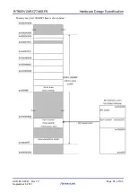
Страница 53: ...5 September 8 2017 RTK00V2XRC7746SFS 4 Memory map 4 1 Specifications Memory map for R Car W2H boot loader is shown below The maximum size of U Boot is the value that subtracted Initialization stack from 240Kbytes The maximum size of initialization stack is 256Kbytes ...

Страница 54: ...e above figure The user area of the code flash memory of the RH850F1H F1L is 2MB A single block of 32 Kbyte extended user area is also incorporated RH8500F1H F1L includes three types of the local RAM Primary local RAM Secondary local RAM Retention RAM RH850 s data memory uses Primary local RAM which is RAM area that can be accessed with speed ...

Страница 55: ...Hardware Design Specification ASD B 16 0247 Rev1 3 Page 55 of 105 September 8 2017 RTK00V2XRC7746SFS Memory map for 32MB SPI flash is shown below ...

Страница 56: ...Hardware Design Specification ASD B 16 0247 Rev1 3 Page 56 of 105 September 8 2017 RTK00V2XRC7746SFS Memory map for 512MB SPI flash is shown below ...

Страница 57: ...7746SFS 4 2 Function These codes of RH850 have realized four functions as follows 4 2 1 Control the power of the Tethys Custom Board The flow chart is as follows Delay 300ms max Pull up SOC_RST END YES NO START Pull down the SOC_RST and SOC_PWRON Pull up SOC_PWRO N SOC_PWRON has been pulled up ...

Страница 58: ...follows Start bit 1 2 3 4 5 6 7 Idle Idle 7 8 or 9 data bits 0 or 1 parity bit 1 or 2 stop bits UART frame RLIN3nTX Figure shows the LIN UART interface in UART mode reception operation as follows 1 2 3 4 5 6 7 Idle Idle 7 8 or 9 data bits 0 or 1 parity bit 1 or 2 stop bits UART frame RLIN3nTX about NSPB IBS s definition please refer to r01uh0445ej0100_rh850f1h pdf page 937 859 s description This U...

Страница 59: ...UART uses RLIN30 of RH850 s LIN UART interface The operations are same as above 4 2 4 Make CAN0 and CAN1 working with baud rate of 1M 1 CAN0 sends 4 byte data only once 2 CAN1 receives the data coming from CAN0 3 Once CAN1 receives the wave form can not be monitored The flow chart is as follows YES END NO START Initialize can0 and can1 Can0 sends 4 byte data Can1 has received the data ...
Страница 60: ...oard dimension The Tethys board dimension is shown as below Unit mm Board 1 6 mm Board 8 Layers Figure 24 The Tethys board dimension 5 2 The weight of the Tethys Board Condition Weight Unit g Screw total 4 Spacer two piece 4 Shell 165 Heat dissipation silica gel 4 Board 143 RF Cable 15cm four piece 16 RF Cable 20cm one piece 5 Tethys assembly total 341 ...

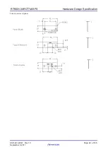
Страница 61: ...e Design Specification ASD B 16 0247 Rev1 3 Page 61 of 105 September 8 2017 RTK00V2XRC7746SFS 5 3 Tethys ID dimension The ID of Tethys board dimension is shown as below Unit mm Base Panel size Cover Panel size ...

Страница 62: ...Hardware Design Specification ASD B 16 0247 Rev1 3 Page 62 of 105 September 8 2017 RTK00V2XRC7746SFS Side Cover size Option ...

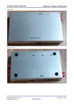
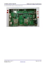
Страница 63: ...dware Design Specification ASD B 16 0247 Rev1 3 Page 63 of 105 September 8 2017 RTK00V2XRC7746SFS 5 4 Tethys assembly The assembly pictures of Tethys board are shown as below Top side view Bottom side view ...

Страница 64: ...Hardware Design Specification ASD B 16 0247 Rev1 3 Page 64 of 105 September 8 2017 RTK00V2XRC7746SFS Top Side View Bottom Side View ...

Страница 65: ...Hardware Design Specification ASD B 16 0247 Rev1 3 Page 65 of 105 September 8 2017 RTK00V2XRC7746SFS Left Side View Right View Side Front Side View Back Side View ...

Страница 66: ...Hardware Design Specification ASD B 16 0247 Rev1 3 Page 66 of 105 September 8 2017 RTK00V2XRC7746SFS V2X RF Cable GPS RF Cable connection image internal AL case ...

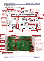
Страница 67: ...RTK00V2XRC7746SFS 6 Board connectors 6 1 TOP side connectors The top side connector is shown as the picture in the following Figure 25 TOP Side Connectors SD Card CN2 GPS CN7 SD Card CN GPS CN DIP Switch Switch LED SW5 SW6 SW7 D9 D7 D5 D3 D11 GPS_LED SW16 SW15 SW14 SW13 SW4 MCU reset ...

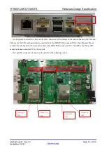
Страница 68: ...ttom side connectors HSM CN CAN Fle xray CN Ethernet CN Audio jack USB CN Micro USB CN16 CN10 CN5 POWER Switch SW18 POWER IN JACK CN17 and CN18 ETNB CN13 MINI PCIE CN DEBUG CN DEBUG CN14 HSM CN14 CAN Flexr ay CN6 Ethernet CN3 Audio jack J1 USB CN1 CN9 CN8 CN12 CN11 POWER Switch POWER IN JACK ETNB CN DIP SW DIP SW DIP SW Micro USB CN LED DIP SW D12 GPS_LED D4 D6 D8 D10 SW12 SW17 SW3 SW1 SW2 SW11 SW...

Страница 69: ...H level CAN bus line 2 CPU_CAN0_L LOW level CAN bus line 3 MCU_CAN0_H HIGH level CAN bus line 4 MCU_CAN0_L LOW level CAN bus line 5 MCU_CAN1_H HIGH level CAN bus line 6 MCU_CAN1_L LOW level CAN bus line 7 BP Flexray bus line plus 8 BM Flexray bus line minus 9 GND Ground 10 GND Ground As the picture shown above there are there USB2UART connectors from the left to right as the figure shown they are ...

Страница 70: ...for the V2X sub board which is inserted in Tethys MINI PCIE connector CN12 the CH0 and CH1 are for the V2X sub board which is inserted in the Tethys MINI PCIE connector CN9 The GPS is for Tethys GPS module antenna connector CN7 at the top side One possible connection is shown as the picture in the following picture CH0 CH1 to V2X SUB CN9 CN12 CN8 CN9 Connect to CH0 Connect to CH1 Connect to CH2 Co...

Страница 71: ...2017 RTK00V2XRC7746SFS 7 Appendix 7 1 USB debug Cable USB debug Cable Length 1 5m This USB cable is used for Micro USB type B connector CN5 CN10 CN16 for debug on V2X main board This cable can be inserted to miniUSB1 miniUSB2 miniUSB3 connector Figure 27 Image of USB debug cable ...

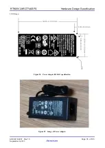
Страница 72: ...cturer GOLDEN PROFIT ELECTRONICS LTD Input voltage range 90 264V AC Input frequency range 63 47 Hz AC input current 1A Max 100V AC AC input power saving 0 075W Max 230V AC at no load Inrush Current 60 A Max 100VAC Cold start 90 A Max 230VAC Cold start Leakage current 0 25mA Max Output voltage 12V Max load current 3A Min load current 0A Output voltage 12 V 5 Output ripple noise 12 V 5 Total output ...

Страница 73: ...Hardware Design Specification ASD B 16 0247 Rev1 3 Page 73 of 105 September 8 2017 RTK00V2XRC7746SFS 7 2 2 Mechanic Size and Picture Mechanic Size Cable Spec ...

Страница 74: ...Hardware Design Specification ASD B 16 0247 Rev1 3 Page 74 of 105 September 8 2017 RTK00V2XRC7746SFS LOG Image Figure 28 Power Adapter ID LOG specification Figure 29 Image of Power Adapter ...

Страница 75: ...aximum 2 0 Bandwidth Minimum 20MHz IF Resister 50ohm Peak Gain 4 dBic base on 70mm x 70mm ground plane Gain coverage 4dBic at 90 θ 90 over 75 volume Polarity RHCP Power consumption 1 watt Gain 30dB typical Noise parameter 1 5dB typical Material Copper Plating treatment Gold plating Male Female Male Filter 24dB 100mHz DC voltage 3 5 0V 0 25V DC current Maximum 16mA Weight 110 g Size 50x50x17 mm3 Ca...

Страница 76: ...6 0247 Rev1 3 Page 76 of 105 September 8 2017 RTK00V2XRC7746SFS This GPS antenna connect the SMA connector labeled GPS in the case Cable Length 5m Figure 30 Image of GPS Antenna from Bottom view Figure 31 Image of GPS Antenna from Top view ...

Страница 77: ...on for V2X 2m cable Item Specification Part Number 6073F00005 Manufacturer Signal Plus Frequency Range 5860 5920MHz Polarization Horizontal Impedance 50 Ohm VSWR 2 0 Max Gain 3 0dBi without cable loss 1 0dBi with cable loss Cable Loss 4 0dB L 2m Radiation Omni Directional Cable length 2m Antenna Cap ABS Color Black Connector SMA Plug Standard Material Copper Plating treatment Gold plating Male Fem...

Страница 78: ...ware Design Specification ASD B 16 0247 Rev1 3 Page 78 of 105 September 8 2017 RTK00V2XRC7746SFS This Antenna s radiation pattern is described as below figures Figure 32 V2X Antenna Test Chamber description ...

Страница 79: ...Hardware Design Specification ASD B 16 0247 Rev1 3 Page 79 of 105 September 8 2017 RTK00V2XRC7746SFS Figure 33 V2X Antennal test axis definition description ...

Страница 80: ...Hardware Design Specification ASD B 16 0247 Rev1 3 Page 80 of 105 September 8 2017 RTK00V2XRC7746SFS Figure 34 V2X Antennal VSWR test character ...

Страница 81: ...Hardware Design Specification ASD B 16 0247 Rev1 3 Page 81 of 105 September 8 2017 RTK00V2XRC7746SFS Figure 35 V2X Antennal 2D radiation pattern ...

Страница 82: ...Hardware Design Specification ASD B 16 0247 Rev1 3 Page 82 of 105 September 8 2017 RTK00V2XRC7746SFS Figure 36 V2X Antennal 3D radiation pattern ...

Страница 83: ...f 105 September 8 2017 RTK00V2XRC7746SFS This V2X antenna connects with the SMA connector labeled CH0 CH1 CH2 CH3 in the case by default while delivery Cable Length 2m Figure 37 Image of V2X Antenna1 from Bottom view Figure 38 Image of V2X Antenna1 from Top view ...

Страница 84: ...ng data Table 29 Antenna Specification for V2X Rod Type Item Specification Part Number 6073F00006 Manufacturer Signal Plus Frequency Range 5860 5920MHz Polarization Vertical Impedance 50 Ohm VSWR 2 0 Max Gain 5 0dBi Cable Loss 0 5dB with SMA Radiation Omni Directional Color Black Connector SMA Plug Standard Material nickel Plating treatment nickel plating Male Female Male Operating Temp 20 65 Stor...

Страница 85: ...are Design Specification ASD B 16 0247 Rev1 3 Page 85 of 105 September 8 2017 RTK00V2XRC7746SFS This Antenna s radiation pattern is described as below figures Figure 39 V2X Antenna2 Test Chamber description ...

Страница 86: ...Hardware Design Specification ASD B 16 0247 Rev1 3 Page 86 of 105 September 8 2017 RTK00V2XRC7746SFS Figure 40 V2X Antenna2 test axis definition description ...

Страница 87: ...Hardware Design Specification ASD B 16 0247 Rev1 3 Page 87 of 105 September 8 2017 RTK00V2XRC7746SFS Figure 41 V2X Antenna2 VSWR test character ...

Страница 88: ...Hardware Design Specification ASD B 16 0247 Rev1 3 Page 88 of 105 September 8 2017 RTK00V2XRC7746SFS Figure 42 V2X Antenna2 2D radiation pattern ...

Страница 89: ...Hardware Design Specification ASD B 16 0247 Rev1 3 Page 89 of 105 September 8 2017 RTK00V2XRC7746SFS Figure 43 V2X Antenna2 3D radiation pattern ...

Страница 90: ...rdware Design Specification ASD B 16 0247 Rev1 3 Page 90 of 105 September 8 2017 RTK00V2XRC7746SFS Figure 44 Image of V2X Antenna2 SMA rotate 90 degree Figure 45 Image of V2X Antenna2 SMA rotate 0 degree ...

Страница 91: ...to the following data Table 30 RF Cable Specification for GPS module RF Board Item Specification Frequency Range 0 6GHz Impedance 50 Ohm VSWR 1 4 Max Cable Loss 1 3dB Max Cable length 1 13 15cm for V2X 2 20cm for GPS Cable Type U FL LP 088 Connector SMA Material Copper Plating treatment Gold plating Male Female Female Operating Temp 40 90 Storage Temp 40 70 Figure 46 RF Cable ...

Страница 92: ...tions Connecter Function Debugger Manufacturer CN1 CPU JTAG ARM JTAG ICE Debugger ARM JTAG ICE Vendor CN4 CPU JTAG2 SH 4AL E10A Renesas Japan CN3 MCU JTAG E1 Renesas Japan Figure 47 JTAG Debug Board with FPC Cable for R CAR W2H RH850 MCU 7 7 2 Block Structure CONN 2 CPU JTAG 02 CPU JTAG2 SH 4AL 02 MCU JTAG 02 Figure 48 JTAG Debug Board block structure ...

Страница 93: ...RST MMC0_D2_TDI MMC0_D1_TMS MMC0_D0_TCK MMC0_D3_ASEBRK ACK 21 1 1634688 4 CN4 0 0 0 0 0 CPU JTAG2 SH 4AL MMC0_CLK_TDO 0 SYS_RESETn_18 13 3 11 9 1 5 7 DCUTRST DCUTDI DCUTMS DCUTCK DCUTDO MCU_RESETn 0 0 0 0 0 0 MCU JTAG 1 1634688 4 CN4 0 0 DCURDY FLMD0 3 7 9 1 5 13 11 4 IMSA 9632S 26Y801 CN2 D1 8V D1 8V BU3 3V BU3 3V D1 8V 26 25 24 23 22 20 6 5 4 3 2 1 19 18 17 16 15 14 13 12 VDD0 VDD1 8 9 8 7 4 7K ...

Страница 94: ...on board This sub board can be connected to CN9 or CN12 to extend SD socket IF Top side view Figure 50 Top side view of V2X Connection board Bottom side view Figure 51 Bottom side view of V2X Connection board 7 8 1 Board Structure GOLD finger 2 CONN 02 Micro SD SLOT 02 Figure 52 Block structure of V2X Connection board ...

Страница 95: ...ger CN1 D3 3V D3 3V RESERVED6 SDIO_DAT2 SDIO_DAT1 SDIO_DAT0 SDIO_CMD SDIO_CLK SDIO_DAT3 SDIO_DAT3 SDIO_DAT2 SDIO_DAT1 SDIO_DAT0 SDIO_CMD SDIO_CLK RESERVED7 RESERVED8 RESERVED9 RESERVED10 RESERVED3 CD DAT3 DAT2 DAT1 DAT0 CMD CLK 3 1 15 13 5 11 Micro SD slot 503182 1852 CN3 RESERVED4 SD_CD PAD VDD PAD 100nF 25V 9 3 3V D3 3V Figure 53 Block Diagram of the V2X Connection board 7 8 3 Block dimension ...

Страница 96: ...e characteristic Min Typ Max Unit Condition Frequency range 5850 5925 MHz Input VSWR 2 0 5890MHz Minimum Sensitivity Diversity off 94 dBm Data rate 3Mbps 93 dBm Data rate 6Mbps 87 dBm Data rate 12Mbps 77 dBm Data rate 27Mbps Minimum Sensitivity Diversity on 94 dBm Data rate 3Mbps 94 dBm Data rate 6Mbps 87 dBm Data rate 12Mbps 80 dBm Data rate 27Mbps Maximum Input Level Diversity off 20 dBm Data ra...

Страница 97: ...ower ANT_A 8 dBm 5890MHz Minimum out put Power ANT_B 7 dBm 5890MHz Minimum out put Power ANT_A 35 dBm 5890MHz Output Power control range 30 dB 5890MHz Power control step 0 5 dB Relative constellation error 28 dB Data rate 3Mbps 28 Data rate 6Mbps 28 Data rate 12Mbps 28 Data rate 27Mbps Spectrum Mask in band 31 dBr 100 KHz 5890 MHz 4 5MHz f 5 0MHz offset Pout 24dBm 33 5 0MHz f 5 5MHz offset Pout 24...

Страница 98: ...Hardware Design Specification ASD B 16 0247 Rev1 3 Page 98 of 105 September 8 2017 RTK00V2XRC7746SFS 7 9 2 Board Dimension ...

Страница 99: ...Hardware Design Specification ASD B 16 0247 Rev1 3 Page 99 of 105 September 8 2017 RTK00V2XRC7746SFS Top Side Bottom Side ...

Страница 100: ...eptember 8 2017 RTK00V2XRC7746SFS 7 10 Side cover option of case AL Case includes the following 2 sets of side cover option which will be used depending on the sub board type which is inserted in CN8 or CN11 connector on Tethys board Figure 54 Side cover option of case ...

Страница 101: ... General Purpose I O HSM Hierarchical Storage Management HSCIF High speed Serial Communication Interface with FIFO I2C Inter Integrated Circuit LED Light Emitting Diode LVTTL Low Voltage Transistor Transistor Logic MCU Microprogrammed Control Unit MMC Multi Media Card PCIE Peripheral Component Interface Express QSPI Queued Serial Peripheral Interface RAM Random Access Memory ROM Read Only Memory S...

Страница 102: ...ct the interference by one of the following measures Reorient or relocate the receiving antenna Increase the separation between the equipment and receiver Connect the equipment into an outlet on a circuit different from that to which the receiver is connected Consult the dealer or an experienced radio TV technician for help NOTE The antenna which installed within the module can t be changed Any an...

Страница 103: ...xposure information The Maximum Permissible Exposure MPE level has been calculated based on a distance of d 20 cm between the device and the human body To maintain compliance with RF exposure requirement use product that maintain a 20cm distance between the device and human body Sound pressure warning Use careful with the earphone maybe possible excessive sound pressure from earphones and headphon...

Страница 104: ... of the radio equipment Model RTK00V2XRC7746SFS is in conformity with the relevant Union harmonization legislation Radio Equipment directive 2014 53 EU and other Union harmonization legislation where applicable N A with reference to the following standards applied EN 60950 1 2006 A11 2009 A1 2010 A12 2011 A2 2013 Draft EN 301 489 1 V2 2 0 2017 03 Final Draft EN 301 489 3 V2 1 1 2017 03 Draft EN 30...

Страница 105: ...D B 16 0247 Rev1 3 Page 105 of 105 September 8 2017 RTK00V2XRC7746SFS 10 Manufacturer Information Manufacturer Shanghai Bwave Technology Co Ltd Address 6F Building 12 399 Keyuan Road Zhangjiang Hi Tech Park City Shanghai Country China ...

Страница 106: ...Website and Support Renesas Electronics Website http www renesas com Inquiries http www renesas com contact ...

Страница 107: ...pin O I 23 25pin O I 31 33pin I O 30pin I I O 2 6pin PO 24 28pin PO 48pin PO GND Remark Power Add FCC CE warning Add No open warning Add CE warning SW11 2 3 not use SW11 2 3 short open 1 2 June 13 2017 All Error in writing correction 1 3 September 8 2017 P104 P105 P106 Change Regulatory Warning Statements Add EU Declaration of Conformity DoC Add Manufacturer Information ...

Страница 108: ...e range heat radiation characteristics installation and other product characteristics Renesas Electronics shall have no liability for malfunctions or damages arising out of the use of Renesas Electronics products beyond such specified ranges 7 Although Renesas Electronics endeavors to improve the quality and reliability of its products semiconductor products have specific characteristics such as t...

Страница 109: ...RTK00V2XRC7746SFS User s Manual Hardware Publication Date Rev 1 3 September 8 2017 Published by Renesas Electronics Corporation ...

Страница 110: ...RTK00V2XRC7746SFS ...

Отзывы: