APPENDIX A REVISION HISTORY
Page 910 of 920
APPENDIX A REVISION HISTORY
A.1
Major Revisions in This Edition
Remark
“Classification” in the above table classifies revisions as follows.
(a): Error correction, (b): Addition/change of specifications, (c): Addition/change of description or note,
(d): Addition/change of package, part number, or management division, (e): Addition/change of related documents
(1/2)
Page
Description
Classification
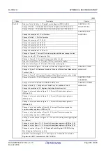
CHAPTER 1 OUTLINE
p.6
Change of Caution in 1.3 Pin Configuration (Top View)
(c)
p.9
Change of 1.6 Outline of Functions
(a)
CHAPTER 3 PIN FUNCTIONS
p.23
Addition of pins to Table 3 - 3 Connection of Unused Pins
(c)
CHAPTER 5 PORT FUNCTIONS
p.93
Change of Table 5 - 11 Setting Examples of Registers When Using P130 to P144 Pin Function
(a)
CHAPTER 6 CLOCK GENERATOR
p.116
Change of Figure 6 - 13 Format of High-speed on-chip oscillator trimming register (HIOTRM)
(a)
p.121
Change of 6.4.4 Low-speed on-chip oscillator
(a)
p.124
Change of 6.6.1 Example of setting high-speed on-chip oscillator
(c)
p.132
Change Notes of Table 6 - 5 CPU Clock Transition and SFR Register Setting Examples (3/5)
(a)
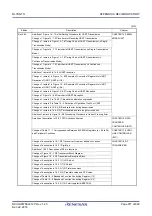
CHAPTER 11 CLOCK OUTPUT/BUZZER OUTPUT CONTROLLER
p.270
Change of Figure 11 - 2 Format of Clock output select registers n (CKSn)
(a)
CHAPTER 12 WATCHDOG TIMER
p.278
Addition of Note to Table 12 - 4 Setting Window Open Period of Watchdog Timer
(c)
CHAPTER 13 A/D CONVERTER
p.309
Change of titles 13.6.4 Hardware trigger no-wait mode (scan mode, one-shot conversion mode)
and Figure 13 - 21 Example of Hardware Trigger No-Wait Mode (Scan Mode, One-Shot Conversion
Mode) Operation Timing
(a)
CHAPTER 14 SERIAL ARRAY UNIT
p.348
Change of 14.3.13 Serial output level register m (SOLm)
(a)
CHAPTER 16 DATA TRANSFER CONTROLLER (DTC)
p.518
Change of Figure 16 - 2 Memory Map Example when DTCBAR Register is Set to FBH
(a)
p.519
Change of Table 16 - 4 Start Address of Control Data
(a)
p.520
Change of Figure 16 - 4 Start Address of Control Data and Vector Table
(a)
CHAPTER 18 RF TRANSCEIVER
p.546
Change of description in 18.2.1 (4) GPIO0/CLKOUT, GPIO1/ANTSELOUT0, GPIO2/ANTSELOUT1,
GPIO3, GPIO4/ANTSW
(c)
p.550
Deletion of description in 18.3.3 (2) RF reference clock output
(b)
p.553
Change of title names of Table 18 - 2 For Normal Receive and Table 18 - 3 For Antenna Diversity
Receive
(c)
p.556
Change of Table 18 - 4 Interrupt Sources List and Note 2, and addition of Note 4
(c)
p.595
Change of Figure 18 - 36 Baseband Interrupt Source Register 1 (BBINTREQ1) Format
(a)
p.596
Change of Figure 18 - 37 Baseband Interrupt Source Register 2 (BBINTREQ2) Format
(a)
Содержание RL78/G1H
Страница 941: ...R01UH0575EJ0120 RL78 G1H...


