


Smart Wi-Fi Module Series
SC20-WL Hardware Design
SC20-WL_Hardware_Design
41 / 81
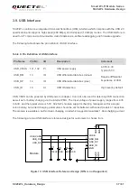
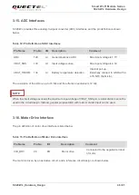
A reference circuit for SD card interface is shown as below.
SD_CMD
120K
NM_51K
SD_DATA3
SD_DATA2
LDO5_1V8
SD_CLK
SD_DATA0
SD_DET
SD_DATA1
P1-DAT2
P2-CD/DAT3
P3-CMD
P4-VDD
P5-CLK
P8-DAT1
GND
P6-VSS
P7-DAT0
DETECTIVE
GND
GND
GND
1
2
3
4
5
6
7
8
9
10
11
12
13
SD_LDO11
33R
33R
33R
33R
33R
33R
1K
2.2uF
SD_LDO12
Module
R1
R2
R3
R4
R5
R6
NM_51K NM_10K NM_51K NM_51K
R7
R8
R9
R10
R11
R12
R13
D1
D2
D3
D4
D5
D6
D7
D8
C1
SD card
connector
Figure 17: Reference Circuit for SD Card Interface
SD_LDO11 is a peripheral driver power supply for SD card. The maximum drive current is approx. 600mA.
Because of the high drive current, it is recommended that the trace width is 0.5mm or more. In order to
ensure the stability of drive power, a 2.2uF capacitor should be added in parallel near the SD card
connector.
CMD, CLK, DATA0, DATA1, DATA2 and DATA3 are all high-speed signal lines. In PCB design, please
control the characteristic impedance of them as 50
Ω, and do not cross with other traces. It is
recommended to route the trace on the inner layer of PCB, and keep the same trace length for CLK, CMD,
DATA0, DATA1, DATA2 and DATA3. CLK additionally needs ground shielding.
Layout guidelines:
C
ontrol impedance as 50Ω±10%, and ground shielding is
required.
The total trace length difference between CLK and other
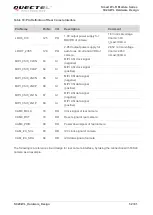
SD_CMD
40
I/O
Command signal of SD card
SD_DATA0
41
I/O
High speed bidirectional
digital signal lines of SD
card
SD_DATA1
42
I/O
SD_DATA2
43
I/O
SD_DATA3
44
I/O
SD_DET
45
DI
SD card insertion detection
Active low