background image

  5G Module Series 

RM505Q-AE Hardware Design


RM505Q-AE_Hardware_Design                                                                                                                  63 / 79


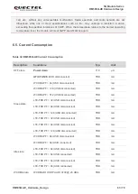
call,  etc.,  without  any  unrecoverable  malfunction.  Radio  spectrum  and  radio  network  are  not 

influenced,  while  one  or  more  specifications,  such  as  P

out

,  may  undergo  a  reduction  in  value, 

exceeding the specified tolerances of 3GPP. When the temperature returns to the normal operating 

temperature level, the module will meet 3GPP specifications again. 


6.5. Current Consumption 


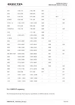
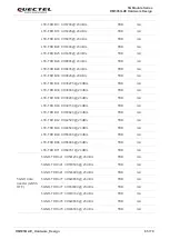
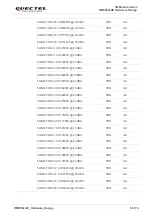
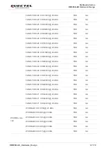
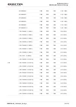
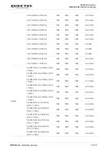
Table 34: RM505Q-AE Current Consumption 

Description 

Conditions 

Typ. 

Unit 

OFF state 

Power down 

71.8               

μA 

Sleep state 

AT+CFUN=0 

(USB disconnected) 

TBD 

mA 

WCDMA PF = 64 (USB disconnected) 

TBD 

mA 

WCDMA PF = 128 (USB disconnected) 

TBD 

mA 

WCDMA PF = 512 (USB disconnected) 

TBD 

mA 

LTE-FDD PF = 32 (USB disconnected) 

TBD 

mA 

LTE-FDD PF = 64 (USB disconnected) 

TBD 

mA 

LTE-FDD PF = 128 (USB disconnected) 

TBD 

mA 

LTE-TDD PF = 32 (USB disconnected) 

TBD 

mA 

LTE-TDD PF = 64 (USB disconnected) 

TBD 

mA 

LTE-TDD PF = 128 (USB disconnected) 

TBD 

mA 

Idle state 

WCDMA PF = 64 (USB disconnected) 

TBD 

mA 

WCDMA PF = 64 (USB connected) 

TBD 

mA 

LTE-FDD PF = 64 (USB disconnected) 

TBD 

mA 

LTE-FDD PF = 64 (USB connected) 

TBD 

mA 

LTE-TDD PF = 64 (USB disconnected) 

TBD 

mA 

LTE-TDD PF = 64 (USB connected) 

TBD 

mA 

WCDMA data 

WCDMA B1 HSDPA CH10700 @ 23 dBm 

TBD 

mA 

Содержание RM505Q-AE

Страница 1: ...RM505Q AE Hardware Design 5G Module Series Version 1 0 0 Date 2020 12 14 Status Preliminary www quectel com ...

Страница 2: ...r notice Disclaimer While Quectel has made efforts to ensure that the functions and features under development are free from errors it is possible that these functions and features could contain errors inaccuracies and omissions Unless otherwise provided by valid agreement Quectel makes no warranties of any kind implied or express with respect to the use of features and functions under development...

Страница 3: ...Quectel Transmitting reproducing disseminating and editing this document as well as using the content without permission are forbidden Offenders will be held liable for payment of damages All rights are reserved in the event of a patent grant or registration of a utility model or design Copyright Quectel Wireless Solutions Co Ltd 2020 All rights reserved ...

Страница 4: ...ardware Design RM505Q AE_Hardware_Design 3 79 About the Document Revision History Version Date Author Description 2020 10 20 Jared WANG Hank LIU Creation of the document 1 0 0 2020 12 14 Jared WANG Simon WANG Hank LIU Preliminary ...

Страница 5: ...Reference Design for Power Supply 24 3 5 Turn on and off Scenarios 25 3 5 1 Turn on the Module 25 3 5 2 Turn off the Module 26 3 5 2 1 Turn off the Module through FULL_CARD_POWER_OFF 26 3 5 2 2 Turn off the Module through AT Command 27 3 6 Reset the Module 27 3 7 U SIM Interfaces 30 3 8 USB Interface 33 3 9 PCIe Interface 35 3 9 1 PCIe Operating Mode 35 3 9 2 USB and PCIe Modes 38 3 10 PCM Interfa...

Страница 6: ...8 5 7 1 Antenna Requirements 58 5 7 2 Recommended RF Connector for Antenna Installation 58 6 Reliability Radio and Electrical Characteristics 61 6 1 Absolute Maximum Ratings 61 6 2 Power Supply Requirements 61 6 3 I O Requirements 62 6 4 Operating and Storage Temperatures 62 6 5 Current Consumption 63 6 6 RF Output Power 68 6 7 RF Receiving Sensitivity 68 6 8 ESD Characteristics 71 6 9 Thermal Dis...

Страница 7: ... the WAKE_ON_WAN Signal 44 Table 18 Function of the DPR Signal 45 Table 19 Pin Definition of COEX Interface 45 Table 20 Pin Definition of Antenna Tuner Control Interface 46 Table 21 Definition of Configuration Pins 47 Table 22 Configuration Pins List of M 2 Specification 47 Table 23 GNSS Performance 48 Table 24 RF Bands Supported by RM505Q AE Antenna Connectors 51 Table 25 RM505Q AE Cellular Anten...

Страница 8: ...uirements of M 2 Specification 37 Figure 20 PCIe Power on Timing Requirements of the Module 37 Figure 21 Primary Mode Timing 39 Figure 22 Auxiliary Mode Timing 40 Figure 23 W_DISABLE1 and W_DISABLE2 Reference Circuit 43 Figure 24 WWAN_LED Reference Circuit 43 Figure 25 WAKE_ON_WAN Signal Reference Circuit 44 Figure 26 Recommended Circuit for Configuration Pins 47 Figure 27 Antenna Connectors on th...

Страница 9: ...5G Module Series RM505Q AE Hardware Design RM505Q AE_Hardware_Design 8 79 Figure 42 Tray Packaging Procedure 76 ...

Страница 10: ...ected with customers applications This document helps you quickly understand the interface specifications electrical and mechanical details as well as other related information of the module To facilitate its application in different fields reference design is also provided for reference Coupled with application notes and user guides you can easily design and set up mobile applications with RM505Q...

Страница 11: ...es may cause interference on sensitive medical equipment so please be aware of the restrictions on the use of wireless devices when in hospitals clinics or other healthcare facilities Cellular terminals or mobiles operating over radio signal and cellular network cannot be guaranteed to connect in certain conditions such as when the mobile bill is unpaid or the U SIM card is invalid When emergent h...

Страница 12: ...ty to meet specific application demands The following table shows the frequency bands and GNSS systems of RM505Q AE module Table 1 Frequency Bands and GNSS Systems of RM505Q AE Module 1 LTE FDD B29 B32 and LTE TDD B46 are supported for receiving only 2 means under development RM505Q AE can be applied in the following fields Rugged tablet PC and laptop computer Remote monitor system Mode RM505Q AE ...

Страница 13: ...2 3 dB for 5G NR n41 n77 n78 n79 bands HPUE 1 5G NR Features 3GPP Rel 15 Modulation Uplink 256QAM Downlink 256QAM Support downlink 4 4 MIMO on n1 n2 n3 n7 25 n38 n40 n41 n48 n66 n77 n78 n79 Support SCS 15 kHz and 30 kHz Support SA and NSA operation modes Support NSA on 5G bands Support SA on 5G bands Support Option 3x 3a and Option 2 NSA TDD Max 2 5 Gbps DL 650 Mbps UL SA TDD Max 2 1 Gbps DL 450 M...

Страница 14: ... output USB serial drivers for Windows 7 8 8 1 10 Linux 2 6 5 4 Android 4 x 5 x 6 x 7 x 8 x 9 x 10 PCIe Interface Complaint with PCIe Gen3 support 8 Gbps per lane Used for AT command communication data transmission firmware upgrade software debugging GNSS NMEA sentence output Rx diversity 5G NR LTE WCDMA Rx diversity GNSS Features Gen9 Lite of Qualcomm Protocol NMEA 0183 Data Update Rate 1 Hz AT C...

Страница 15: ...ensure effective thermal dissipation for example by adding passive or active heatsinks heat pipes vapor chambers etc Within this range the module remains the ability to establish and maintain functions such as voice SMS emergency call etc without any unrecoverable malfunction Radio spectrum and radio network are not influenced while one or more specifications such as Pout may undergo a reduction i...

Страница 16: ...ace FULL_CARD_POWER_OFF W_DISABLE2 USB 2 0 USB 3 1 U SIM1 WWAN_LED WAKE_ON_WAN 4Gb NAND 4Gb x8 4Gb LPDDR4X SDRAM 4Gb x16 RFFE W_DISABLE1 GPIOs Tx Rx Blocks ANT1 PCIe 1 U SIM2 GND ANT4_GNSS Figure 1 Functional Block Diagram 2 4 Evaluation Board To help you develop applications conveniently with RM505Q AE Quectel supplies an evaluation board PCIe Card EVB a USB to RS 232 converter cable a USB type C...

Страница 17: ...ply with PCI Express M 2 specification This chapter mainly describes the definition and application of the following interfaces pins of RM505Q AE Power supply U SIM interfaces USB interface PCIe interface PCM interface Control and indication interfaces Cellular WLAN COEX interface Antenna tuner control interface Configuration pins means under development NOTE ...

Страница 18: ...39 USB_SS_RX_P 37 USB_SS_RX_M 35 GND 33 USB_SS_TX_P 31 USB_SS_TX_M 29 GND 27 DPR 25 WAKE_ON_WAN 23 CONFIG_0 21 Notch Notch Notch Notch GND 11 USB_DM 9 USB_DP 7 GND 5 GND 3 CONFIG_3 1 PIN11 PIN10 No Pin Name 74 VCC 72 VCC 70 VCC 68 AP2SDX_STATUS 66 USIM1_DET 64 COEX_TXD 62 COEX_RXD 60 WLAN_TX_EN 58 RFFE_DATA 56 RFFE_CLK 54 PCIE_WAKE_N 52 PCIE_CLKREQ_N 50 PCIE_RST_N 48 USIM2_VDD 46 USIM2_RST 44 USIM...

Страница 19: ...ut DI Digital Input DO Digital Output IO Bidirectional OD Open Drain PI Power Input PO Power Output Pin No Pin Name I O Description Comment 1 CONFIG_3 DO Not connected internally 2 VCC PI Power supply for the module Vmin 3 135 V Vnorm 3 7 V Vmax 4 4 V 3 GND Ground 4 VCC PI Power supply Vmin 3 135 V Vnorm 3 7 V Vmax 4 4 V 5 GND Ground 6 FULL_CARD_POWER_ OFF DI Turn on off of the module Internally p...

Страница 20: ...ndication LED Open drain and active low signal 11 GND Ground 12 Notch Notch 13 Notch Notch 14 Notch Notch 15 Notch Notch 16 Notch Notch 17 Notch Notch 18 Notch Notch 19 Notch Notch 20 PCM_CLK IO PCM data bit clock 1 8 V power domain 21 CONFIG_0 DO Not connected internally 22 PCM_DIN DI PCM data input 1 8 V power domain 23 WAKE_ON_WAN OD Wake up the host Open drain Active LOW 24 PCM_DOUT DO PCM dat...

Страница 21: ...wer domain 37 USB_SS_RX_P AI USB 3 1 super speed receive Requires differential impedance of 90 Ω 38 SDX2AP_STATUS DO Status indication to AP 1 8 V power domain 39 GND Ground 40 USIM2_DET DI U SIM2 card insertion detection Internally pulled up to 1 8 V 41 PCIE_TX_M AO PCIe transmit Requires differential impedance of 85 Ω 42 USIM2_DATA IO U SIM2 card data 1 8 3 0 V power domain 43 PCIE_TX_P AO PCIe ...

Страница 22: ...DO Notification from SDR to WLAN when transmitting via LTE 1 8 V power domain 60 WLAN_TX_EN DI Notification from WLAN to SDR while transmitting 1 8 V power domain 61 ANTCTL DO Antenna control 1 8 V power domain 62 COEX_RXD DI LTE WLAN coexistence receive 1 8 V power domain 63 ANTCTL DO Antenna control 1 8 V power domain 64 COEX_TXD DO LTE WLAN coexistence transmit 1 8 V power domain 65 RFFE_VIO_1V...

Страница 23: ...Software is active The module has registered on the network and it is ready to send and receive data Talk Data The module is connected to network In this mode the power consumption is decided by network setting and data transfer rate Minimum Functionality Mode AT CFUN 0 command sets the module to a minimum functionality mode without removing the power supply In this mode both RF function and U SIM...

Страница 24: ...capacitor of about 100 µF with low ESR ESR 0 7 Ω should be used and a multi layer ceramic chip capacitor MLCC array should also be used due to its ultra low ESR It is recommended to use four ceramic capacitors 1 µF 100 nF 33 pF 10 pF for composing the MLCC array and place these capacitors close to VCC pins The width of VCC trace should be no less than 2 0 mm In principle the longer the VCC trace i...

Страница 25: ...red output VCC 3 7 V typical a buck DC DC converter is preferred as the power supply The following figure shows a reference design for 5 0 V input power source based on the DC DC converter The typical output of the power supply is about 3 7 V and the maximum load current is 3 0 A D1 TVS PWR_IN C8 220 μF C11 10 pF C10 33 pF C9 100 nF R1 205k U1 Q1 NPN R8 47k R7 4 7k PWR_EN R4 182k PWR_OUT L1 1 5 μH...

Страница 26: ...table shows the definition of FULL_CARD_POWER_OFF Table 7 Definition of FULL_CARD_POWER_OFF Pin The timing of turn on scenario is illustrated in the following figure VCC RESET_N Module power on or insertion detection USIM1_VDD USIM2_VDD Module Status FULL_CARD_POWER_OFF RFFE_VIO_1V8 System turn on and booting VIH 1 19 V 1 8 V or 3 0 V System booting Inactive Active tpower on tturn on tbooting 68 m...

Страница 27: ...st device 2 tturn on is the interval between FULL_CARD_POWER_OFF high voltage level and RFFE_VIO_1V8 an internal LDO output high voltage level which is typically 68 ms 3 t0 is the interval between VCC and FULL_CARD_POWER_OFF high voltage level FULL_CARD_POWER_OFF could be pulled up at any time decided by the host as shown in figure above 4 tbooting is the interval between RFFE_VIO_1V8 high voltage...

Страница 28: ... For more details about the command see document 2 The module is designed to be turned on with a host GPIO Pull down FULL_CARD_POWER_OFF pin after the module s USB PCIe is removed otherwise the module will be powered on again VCC FULL_CARD_POWER_OFF RUNNING OFF Module Status Turn off procedure RESET_N H USB PCIe AT QPOWD USB PCIe removed Figure 9 Turn off Timing through AT Command and FULL_CARD_PO...

Страница 29: ...ble 8 Definition of RESET_N Pin The module can be reset by pulling down the RESET_N pin for 200 700 ms You can use an open collector drain driver or button to control RESET_N pin Host Module RESET_N Reset Logic GPIO 67 VDD 1 5 V Reset pulse 200 700 ms R1 100k R3 100k R2 1k Q1 NPN Figure 10 Reference Circuit for RESET_N with NPN Driving Circuit Pin No Pin Name Description DC Characteristics Comment...

Страница 30: ...R1 100K R5 100K R4 10R Q2 NMOS Figure 11 Reference Circuit for RESET_N with NMOS Driving Circuit Module RESET_N Reset Logic 67 VDD 1 5 V 200 700 ms S1 TVS R1 100K 33 pF C1 Note The capacitor C1 is recommended to be less than 47 pF Figure 12 Reference Circuit for RESET_N with Button The timing of reset scenario is illustrated in the following figure ...

Страница 31: ...ption Comment 36 USIM1_VDD PO Power supply for U SIM1 card Class B 3 0 V and Class C 1 8 V 34 USIM1_DATA IO U SIM1 card data 1 8 3 0 V power domain 32 USIM1_CLK DO U SIM1 card clock 1 8 3 0 V power domain 30 USIM1_RST DO U SIM1 card reset 1 8 3 0 V power domain 66 USIM1_DET DI U SIM1 card insertion detection Internally pulled up to 1 8 V 48 USIM2_VDD PO Power supply for U SIM2 card Class B 3 0 V a...

Страница 32: ...T is at low voltage level When the U SIM is inserted CD is open from ground and USIM_DET is at high voltage level The following figure shows a reference design of U SIM interface with a normally closed U SIM card connector Module U SIM Card Connector USIM_DET USIM_DATA USIM_CLK RST CLK CD IO USIM_VDD USIM_VDD USIM_RST VCC GND VPP GND TVS Note All these resistors capacitors and TVS should be close ...

Страница 33: ...ollowing figure Module U SIM Card Connector USIM_DET USIM_DATA USIM_CLK RST CLK IO USIM_VDD USIM_VDD USIM_RST VCC GND VPP GND TVS Note All these resistors capacitors and TVS should be close to U SIM card connector in PCB layout 10 20k 22R 22R 22R 33 pF 33 pF 33 pF 100 nF Figure 16 Reference Circuit for a 6 Pin U SIM Card Connector To enhance the reliability and availability of the U SIM card in ap...

Страница 34: ...ule provides one integrated Universal Serial Bus USB interface which complies with the USB 3 1 2 0 specifications and supports super speed 10 Gbps on USB 3 1 and high speed 480 Mbps and full speed 12 Mbps modes on USB 2 0 The USB interface is used for AT command communication data transmission GNSS NMEA sentence output software debugging firmware upgrade Note that only USB 2 0 can be used for firm...

Страница 35: ...ou should follow the principles below when designing for the USB interface to meet USB 3 1 and 2 0 specifications Route the USB signal traces as differential pairs with ground surrounded The impedance of differential trace of USB 2 0 and 3 1 is 90 Ω For USB 2 0 signal traces the trace length should be less than 120 mm and the differential data pair matching should be less than 2 mm For USB 3 1 sig...

Страница 36: ...nd root complex RC mode In EP mode the module is configured as a PCIe EP device In RC mode the module is configured as a PCIe root complex The following figure shows a reference circuit for the PCIe interface Pin No Pin Name I O Description Comment 55 PCIE_REFCLK_P AI AO PCIe reference clock 100 MHz Requires differential impedance of 85 Ω 53 PCIE_REFCLK_M AI AO PCIe reference clock 49 PCIE_RX_P AI...

Страница 37: ...vel of VCC_IO_HOST depends on the host side due to the open drain in pins 50 52 and 54 C6 220 nF C5 220 nF C2 220 nF C1 220 nF R1 100k R2 100k R3 100k VCC_IO_HOST R5 0R R4 0R Figure 18 PCIe Interface Reference Circuit AT QCFG pcie mode is used to set PCIe RC EP mode For more details about the command see document 2 To ensure the signal integrity of PCIe interface AC coupling capacitors C5 and C6 s...

Страница 38: ... PCIe Power on Timing Requirements of the Module The following principles of PCIe interface design should be complied with so as to meet PCIe specification Keep the PCIe data and control signals away from sensitive circuits and signals such as RF audio crystal and oscillator signals Add a capacitor in series on Tx Rx traces to prevent any DC bias Keep the maximum trace length less than 300 mm Keep...

Страница 39: ... Communication can be switched back to USB mode by AT command When RM505Q AE module works at the USB AT based switched from USB mode by AT command PCIe mode it supports MBIM QMI QRTR AT and can be switched back to USB mode by AT command But the firmware upgrade via PCIe interface is not supported so USB 2 0 interface must be reserved for the firmware upgrade eFuse based PCIe Mode Supports MBIM QMI...

Страница 40: ... the PCM interface supports 256 kHz 512 kHz 1024 kHz or 2048 kHz PCM_CLK at 8 kHz PCM_SYNC and also supports 4096 kHz PCM_CLK at 16 kHz PCM_SYNC In the auxiliary mode the data is sampled on the falling edge of the PCM_CLK and transmitted on the rising edge The PCM_SYNC rising edge represents the MSB In this mode PCM interface operates with a 256 kHz PCM_CLK and an 8 kHz PCM_SYNC of 50 duty cycle o...

Страница 41: ...by AT command and the default configuration is master mode using short frame synchronization format with 2048 kHz PCM_CLK and 8 kHz PCM_SYNC See document 2 for details about AT QDAI command means under development Pin No Pin Name I O Description Comment 20 PCM_CLK IO PCM data bit clock 1 8 V power domain In master mode it is an output signal In slave mode it is an input signal If unused keep it op...

Страница 42: ...RF function can also be enabled or disabled through software method that is through AT commands The following table shows the AT command and corresponding RF function status of the module Pin No Pin Name I O Description Comment 8 W_DISABLE1 DI Airplane mode control 1 8 3 3 V power domain Active LOW 10 WWAN_LED OD Indicate RF status of the module Open drain and active low signal 23 WAKE_ON_WAN OD W...

Страница 43: ...based on diodes is used on W_DISABLE1 pin and W_DISABLE2 pin which are pulled up to a 1 8 V voltage in the module as shown in the following figure So the control signals GPIO of the host device could be a 1 8 V or 3 3 V voltage level Signals from W_DISABLE1 and W_DISABLE2 are active low and a reference circuit is presented below W_DISABLE1 Logic Level AT Commands RF Function Status High AT CFUN 1 ...

Страница 44: ...ED The WWAN_LED signal is used to indicate the RF status of the module and its sink current is up to 10 mA To reduce current consumption of the LED a current limited resistor must be placed in series with the LED as illustrated in the figure below The LED is ON when the WWAN_LED signal is at low voltage level Host Module WWAN_LED PMU GPIO 10 VCC Note This VCC could be the power supply of the modul...

Страница 45: ...e WAKE_ON_WAN BB GPIO 23 VCC_IO_HOST Note The voltage level on VCC_IO_HOST depends on the host side due to the open drain in pin 23 Wake up the host 1s H L R1 10k Figure 25 WAKE_ON_WAN Signal Reference Circuit WWAN_LED Logic Level Description Low LED on RF function is turned on High LED off RF function is turned off if any of the following occurs The U SIM card is not powered W_DISABLE1 is at low ...

Страница 46: ... IPQ807x device Pin 38 SDX2AP_STATUS outputs the status indication signal to IPQ807x device and pin 68 AP2SDX_STATUS inputs the status indication signal from IPQ807x device 3 12 Cellular WLAN Interface RM505Q AE provides a cellular WLAN COEX interface the following table shows the pin definition of this interface Table 19 Pin Definition of COEX Interface DPR Level Function High Floating NO max tra...

Страница 47: ...he interface will be added in the future version of this document Table 20 Pin Definition of Antenna Tuner Control Interface means under development 60 WLAN_TX_EN DI Notification from WLAN to SDR while transmitting 1 8 V power domain Pin No Pin Name I O Description DC Characteristics 56 RFFE_CLK DO Used for external MIPI IC control VOLmax 0 45 V VOHmin 1 35 V VOHmax 1 8 V 58 RFFE_DATA DO 61 ANTCTL...

Страница 48: ... 10K NM 0 Ω NM 0 Ω NM 0 Ω 0 Ω Note The voltage level of VCC_IO_HOST depends on the host side and could be 1 8 V or 3 3 V Figure 26 Recommended Circuit for Configuration Pins Table 22 Configuration Pins List of M 2 Specification Pin No Pin Name I O Power Domain Description 21 CONFIG_0 DO 0 Not connected internally 69 CONFIG_1 DO 0 Connected to GND internally 75 CONFIG_2 DO 0 Not connected internall...

Страница 49: ...te via USB interface by default The GNSS engine is switched off by default It has to be switched on via AT command For more details about GNSS engine technology and configurations see document 3 4 2 GNSS Performance The following table shows GNSS performance of the module Table 23 GNSS Performance Parameter Description Conditions Typ Unit Sensitivity GNSS Cold start Autonomous TBD dBm Reacquisitio...

Страница 50: ...inuously 2 Reacquisition sensitivity the minimum GNSS signal power required for the module to maintain locked within 3 minutes after the loss of lock 3 Cold start sensitivity the minimum GNSS signal power at which the module can fix position successfully within 3 minutes after executing cold start command Hot start open sky Autonomous TBD s XTRA enabled TBD s Accuracy GNSS CEP 50 Autonomous open s...

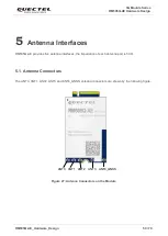
Страница 51: ...a Interfaces RM505Q AE provides five antenna interfaces the impedance of each antenna port is 50 Ω 5 1 Antenna Connectors The ANT0 ANT1 ANT2 ANT3 and ANT4_GNSS antenna connectors are shown by the following figure ANT0 ANT1 ANT3 ANT2 ANT4_GNSS Figure 27 Antenna Connectors on the Module ...

Страница 52: ...O LTE B46 PRx LTE UHB DRx MIMO 5G FDD LB TRx0 5G FDD TDD MHB DRx MIMO 5G NR n77 n78 n79 DRx MIMO 50 Ω impedance ANT2 AI AO LTE LB DRx LTE MHB PRx MIMO 5G NR n77 n78 n41 n79 TRx0 LTE UHB TRx0 5G FDD LB DRx 5G FDD MHB PRx MIMO 50 Ω impedance ANT3 AI AO LTE MHB DRx LTE B46 DRx LTE UHB DRx 5G FDD TDD MHB DRx 5G NR n77 n78 n79 DRx 50 Ω impedance ANT4_ GNSS AI GNSS L1 L5 Rx 50 Ω impedance Pin Name I O D...

Страница 53: ...TE B46 DRx LTE UHB DRx 5G FDD TDD MHB DRx 5G NR n77 n78 n79 DRx 50 Ω impedance ANT4_ GNSS AI GNSS L1 L5 Rx 50 Ω impedance Band Name Transmit MHz Receive MHz LTE FDD LTE TDD UMTS 5G NR IMT 2100 1920 1980 2110 2170 B1 B1 n1 PCS 1900 1850 1910 1930 1990 B2 B2 n2 DCS 1800 1710 1785 1805 1880 B3 B3 n3 AWS 1710 1755 2110 2155 B4 B4 Cell 850 824 849 869 894 B5 B5 n5 JCELL 800 830 840 875 885 B6 IMT E 260...

Страница 54: ...59 894 B26 700 APAC 703 748 758 803 B28 n28 FLO 717 728 B29 WCS 2305 2315 2350 2360 B30 L band 1452 1496 B32 B34 2010 2025 2010 2025 B34 B38 2570 2620 2570 2620 B38 n38 B39 1880 1920 1880 1920 B39 B40 2300 2400 2300 2400 B40 n40 B41 B41 XGP 2496 2690 2496 2690 B41 n41 B42 3400 3600 3400 3600 B42 B43 3600 3800 3600 3800 B43 B46 5150 5925 5150 5925 B46 B48 3550 3700 3550 3700 B48 n48 B66 1710 1780 2...

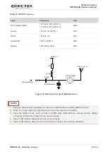
Страница 55: ...tching components as close to the antenna as possible 3 Keep the digital circuits such as that of U SIM card USB interface camera module display connector and SD card away from the antenna traces 4 Keep 75 dB isolation between each two antenna traces 5 Keep 15 dB isolation between each two antenna to improve the receiving sensitivity Type Frequency Unit GPS Galileo QZSS 1575 42 1 023 GPS L1 1176 4...

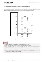
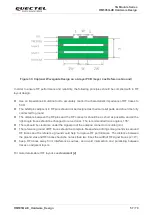
Страница 56: ...T3 ANT4_GNSS 0R 0R 0R Figure 29 Reference Design for Cellular Antenna 1 Keep the characteristic impedance for cellular antenna traces to 50 Ω 2 Place the π type matching components as close to the antenna as possible 3 Keep the digital circuits such as that of U SIM card USB interface camera module display connector and SD card away from the antenna traces 4 Keep 75 dB PCB isolation between two an...

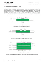
Страница 57: ...c constant the height from the reference ground to the signal layer H and the spacing between RF traces and grounds S Microstrip or coplanar waveguide is typically used in RF layout to control characteristic impedance The following are reference designs of microstrip or coplanar waveguide with different PCB structures Figure 30 Microstrip Design on a 2 layer PCB Figure 31 Coplanar Waveguide Design...

Страница 58: ...e between the RF pins and the RF connector should be as short as possible and all the right angle traces should be changed to curved ones The recommended trace angle is 135 There should be clearance under the signal pin of the antenna connector or solder joint The reference ground of RF traces should be complete Meanwhile adding some ground vias around RF traces and the reference ground could help...

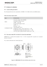
Страница 59: ...s mounted with standard 2 0 mm 2 0 mm receptacle RF connectors for convenient antenna connection The connector dimensions are illustrated as below Figure 34 RM505Q AE RF Connector Dimensions Unit mm Type Requirements GNSS Frequency range 1559 1606 MHz Polarization RHCP or linear VSWR 2 typical Passive antenna gain 0 dBi WCDMA LTE 5G NR VSWR 3 Efficiency 30 Input Impedance 50 Ω WCDMA LB LTE LB Cabl...

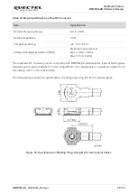
Страница 60: ...m using a Ø 0 81 mm coaxial cable or a maximum height of 1 45 mm utilizing a Ø 1 13 mm coaxial cable The following figure shows the specifications of mating plugs using Ø 0 81 mm coaxial cables Figure 35 Specifications of Mating Plugs Using Ø 0 81 mm Coaxial Cables Item Specification Nominal Frequency Range DC to 6 GHz Nominal Impedance 50 Ω Temperature Rating 40 C to 85 C Voltage Standing Wave Ra...

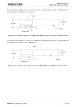
Страница 61: ...nd the mating plug using a Ø 0 81 mm coaxial cable Figure 36 Connection between RF Connector and Mating Plug Using Ø 0 81 mm Coaxial Cable The following figure illustrates the connection between the receptacle RF connector on RM505Q AE and the mating plug using a Ø 1 13 mm coaxial cable Figure 37 Connection between RF Connector and Mating Plug Using Ø 1 13 mm Coaxial Cable ...

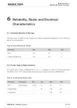
Страница 62: ...ng table Table 30 Absolute Maximum Ratings 6 2 Power Supply Requirements The typical input voltage of RM505Q AE is 3 7 V as specified by PCIe M 2 Electromechanical Specification Rev 1 0 The following table shows the power supply requirements of RM505Q AE Table 31 Power Supply Requirements Parameter Min Max Unit VCC 0 3 4 7 V Voltage at Digital Pins 0 3 2 3 V Parameter Description Min Typ Max Unit ...

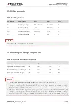
Страница 63: ...tc Within this range the module meets 3GPP specifications 3 2 To meet this extended temperature range you need to ensure effective thermal dissipation for example by adding passive or active heatsinks heat pipes vapor chambers etc Within this range the module remains the ability to establish and maintain functions such as voice SMS emergency Parameter Description Min Max Unit VIH Input high voltag...

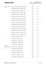
Страница 64: ...s Typ Unit OFF state Power down 71 8 μA Sleep state AT CFUN 0 USB disconnected TBD mA WCDMA PF 64 USB disconnected TBD mA WCDMA PF 128 USB disconnected TBD mA WCDMA PF 512 USB disconnected TBD mA LTE FDD PF 32 USB disconnected TBD mA LTE FDD PF 64 USB disconnected TBD mA LTE FDD PF 128 USB disconnected TBD mA LTE TDD PF 32 USB disconnected TBD mA LTE TDD PF 64 USB disconnected TBD mA LTE TDD PF 12...

Страница 65: ...23 dBm TBD mA WCDMA B6 HSDPA CH4400 23 dBm TBD mA WCDMA B6 HSUPA CH4400 23 dBm TBD mA WCDMA B8 HSDPA CH3012 23 dBm TBD mA WCDMA B8 HSUPA CH3012 23 dBm TBD mA WCDMA B19 HSDPA CH738 23 dBm TBD mA WCDMA B19 HSUPA CH738 23 dBm TBD mA LTE data transfer GNSS OFF LTE FDD B1 CH300 23 dBm TBD mA LTE FDD B2 CH900 23 dBm TBD mA LTE FDD B3 CH1575 23 dBm TBD mA LTE FDD B4 CH2175 23 dBm TBD mA LTE FDD B5 CH2525...

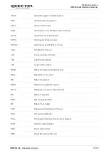
Страница 66: ...BD mA LTE TDD B39 CH38450 23 dBm TBD mA LTE TDD B40 CH39150 23 dBm TBD mA LTE TDD B41 CH40620 23 dBm TBD mA LTE TDD B42 CH42590 23 dBm TBD mA LTE TDD B43 CH44590 23 dBm TBD mA LTE TDD B48 CH55990 23 dBm TBD mA LTE FDD B66 CH66886 23 dBm TBD mA LTE FDD B71 CH68761 23 dBm TBD mA 5G NR data transfer GNSS OFF 5G NR TDD n41 CH501204 23 dBm TBD mA 5G NR TDD n41 CH518598 23 dBm TBD mA 5G NR TDD n41 CH535...

Страница 67: ... FDD n2 CH397000 23 dBm TBD mA 5G NR FDD n3 CH362000 23 dBm TBD mA 5G NR FDD n3 CH368500 23 dBm TBD mA 5G NR FDD n3 CH375000 23 dBm TBD mA 5G NR FDD n5 CH174800 23 dBm TBD mA 5G NR FDD n5 CH176300 23 dBm TBD mA 5G NR FDD n5 CH177800 23 dBm TBD mA 5G NR FDD n7 CH525000 23 dBm TBD mA 5G NR FDD n7 CH531000 23 dBm TBD mA 5G NR FDD n7 CH537000 23 dBm TBD mA 5G NR FDD n8 CH186000 23 dBm TBD mA 5G NR FDD...

Страница 68: ...mA 5G NR TDD n38 CH519000 23 dBm TBD mA 5G NR TDD n38 CH523000 23 dBm TBD mA 5G NR TDD n40 CH461000 23 dBm TBD mA 5G NR TDD n40 CH470000 23 dBm TBD mA 5G NR TDD n40 CH479000 23 dBm TBD mA 5G NR FDD n66 CH423000 23 dBm TBD mA 5G NR FDD n66 CH429000 23 dBm TBD mA 5G NR FDD n66 CH435000 23 dBm TBD mA 5G NR FDD n71 CH124400 23 dBm TBD mA 5G NR FDD n71 CH126900 23 dBm TBD mA 5G NR FDD n71 CH129400 23 d...

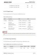
Страница 69: ... receiving sensitivity of RM505Q AE module Table 36 RM505Q AE Conducted RF Receiving Sensitivity WCDMA B8 CH3012 23 dBm TBD mA WCDMA B19 CH338 23 dBm TBD mA Mode Frequency Max Min WCDMA WCDMA bands 24 dBm 1 3 dB Class 3 50 dBm LTE LTE bands 23 dBm 2 dB Class 3 40 dBm LTE HPUE bands B38 B40 B41 B42 B43 26 dBm 2 dB Class 2 40 dBm 5G NR 5G NR bands 23 dBm 2 dB Class 3 40 dBm BW 5 20 MHz 1 5G NR HPUE ...

Страница 70: ...BD TBD 96 3 dBm LTE FDD B5 10 MHz TBD TBD TBD 94 3 dBm LTE FDD B7 10 MHz TBD TBD TBD 94 3 dBm LTE FDD B8 10 MHz TBD TBD TBD 93 3 dBm LTE FDD 10 MHz TBD TBD TBD 95 3 dBm LTE FDD B12 10 MHz TBD TBD TBD 93 3 dBm LTE FDD B13 10 MHz TBD TBD TBD 93 3 dBm LTE FDD B14 10 MHz TBD TBD TBD 93 3 dBm LTE FDD B17 10 MHz TBD TBD TBD 93 3 dBm LTE FDD B18 10 MHz TBD TBD TBD 96 3 dBm LTE FDD B19 10 MHz TBD TBD TBD ...

Страница 71: ...E FDD B71 10 MHz TBD TBD TBD 94 2 dBm 5G NR 5G NR FDD n1 20 MHz SCS 15 kHz TBD TBD TBD 94 0 dBm 5G NR FDD n2 20 MHz SCS 15 kHz TBD TBD TBD 92 0 dBm 5G NR FDD n3 20 MHz SCS 15 kHz TBD TBD TBD 91 0 dBm 5G NR FDD n5 10 MHz SCS 15 kHz TBD TBD TBD 95 0 dBm 5G NR FDD n7 20 MHz SCS 15 kHz TBD TBD TBD 92 0 dBm 5G NR FDD n8 10 MHz SCS 15 kHz TBD TBD TBD 94 0 dBm 5G NR FDD n12 10 MHz SCS 15 kHz TBD TBD TBD ...

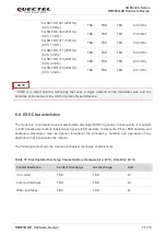
Страница 72: ...hout the processing handling and operation of any application that incorporates the module The following table shows the module electrostatic discharge characteristics Table 37 Electrostatic Discharge Characteristics Temperature 25 º C Humidity 40 5G NR TDD n41 20 MHz SCS 30 kHz TBD TBD TBD 92 0 dBm 5G NR FDD n66 20 MHz SCS 15 kHz TBD TBD TBD 93 5 dBm 5G NR FDD n71 10 MHz SCS 15 kHz TBD TBD TBD 94...

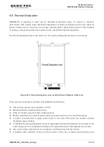
Страница 73: ...oth Sides of Module Unit mm There are other measures to enhance heat dissipation performance Add as many ground vias as possible on PCB Maximize airflow over around the module Place the module away from other heating sources Module mounting holes must be used to attach ground the device to the main PCB ground It is NOT recommended to apply solder mask on the main PCB where the module s thermal dis...

Страница 74: ... and the heatsink should be designed with as many fins as possible to increase the heat dissipation area If a conformal coating is necessary for the module do NOT use any coating material that may chemically react with the PCB or shielding cover and prevent the coating material from flowing into the module NOTE ...

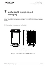
Страница 75: ... and Packaging This chapter mainly describes mechanical dimensions and packaging specifications of RM505Q AE module All dimensions are measured in mm and the tolerances are 0 05 mm unless otherwise specified 7 1 Mechanical Dimensions of the Module Figure 39 Mechanical Dimensions of RM505Q AE Unit mm ...

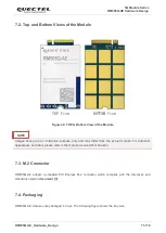
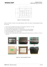
Страница 76: ...for illustration purpose only and may differ from the actual module For authentic appearance and label please refer to the module received from Quectel 7 3 M 2 Connector RM505Q AE adopts a standard PCI Express M 2 connector which compiles with the directives and standards listed in document 5 7 4 Packaging RM505Q AE modules are packaged in trays The following figure shows the tray size NOTE ...

Страница 77: ...ge 100 modules at a time tray size 247 mm 172 mm 2 Place an empty tray on the top of the 10 tray stack 3 Fix the stack with masking tape in shape as shown in the following figure 4 Pack the stack with conductive bag and then fix the bag with masking tape 5 Place the list of IMEI No into a small carton 6 Seal the carton and then label the seal with sealing sticker small carton size 250 mm 175 mm 12...

Страница 78: ...xxQ_Series_GNSS_Application_ Note The GNSS application note for RG50xQ and RM5xxQ series 4 Quectel_RF_Layout_Application_Note RF layout application note 5 PCI Express M 2 Specification Revision 3 0 PCI express M 2 specification Abbreviation Description bps Bit Per Second COEX Coexistence DFOTA Delta Firmware Upgrade Over The Air DL Downlink DPR Dynamic Power Reduction EIRP Equivalent Isotropically...

Страница 79: ...ps Kilo Bits Per Second LAA License Assisted Access LED Light Emitting Diode LTE Long Term Evolution MBIM Mobile Broadband Interface Model Mbps Mega Bits Per Second ME Mobile Equipment MIMO Multiple Input Multiple Output MLCC Multiplayer Ceramic Chip Capacitor MO Mobile Originated MSB Most Signification Bit MT Mobile Terminated PAP Password Authentication Protocol PCB Printed Circuit Board PCIe Pe...

Страница 80: ...ver Transmitter UL Uplink URC Unsolicited Result Code USB Universal Serial Bus U SIM Universal Subscriber Identity Module VIH Input High Voltage Level VIL Input Low Voltage Level VOH Output High Voltage Level VOL Output Low Voltage Level WCDMA Wideband Code Division Multiple Access WLAN Wireless Local Area Network and must not transmit simultaneously with any other antenna or transmitter The EUT i...

Страница 81: ...onal emissions other than what is permitted in Part 15 Subpart B or emissions are complaint with the transmitter s rule s The Grantee will provide guidance to the host manufacturer for Part 15 B requirements if needed Important Note notice that any deviation s from the defined parameters of the antenna trace as described by the instructions require that the host product manufacturer must notify to...

Страница 82: ...imum antenna gain including cable loss must not exceed Test Mode Antenna Gain dBi Test Mode Antenna Gain dBi WCDMA B2 8 00 LTE B38 2 00 WCDMA B4 5 00 LTE B41 2 00 WCDMA B5 5 00 LTE B48 2 00 LTE B2 8 00 LTE B66 5 00 LTE B4 5 00 LTE B71 5 00 LTE B5 5 00 n2 8 00 LTE B7 8 00 n5 5 00 LTE B12 5 00 n7 8 00 LTE B13 5 00 n12 5 00 LTE B14 5 00 n25 8 00 LTE B17 5 00 n41 5 00 LTE B25 8 00 n66 5 00 LTE B26 5 0...

Страница 83: ...asures Reorient or relocate the receiving antenna Increase the separation between the equipment and receiver Connect the equipment into an outlet on a circuit different from that to which the receiver is connected Consult the dealer or an experienced radio TV technician for help Any changes or modifications not expressly approved by the party responsible for compliance could void the user s author...

Страница 84: ...nna As long as 2 conditions above are met further transmitter test will not be required However the OEM integrator is still responsible for testing their end product for any additional compliance requirements required with this module installed Radiation Exposure Statement This equipment complies with FCC radiation exposure limits set forth for an uncontrolled environment This equipment should be ...

Страница 85: ...its set forth for an uncontrolled environment This equipment should be installed and operated with minimum distance 20 cm between the radiator your body Déclaration d exposition aux radiations Cet équipement est conforme aux limites d exposition aux rayonnements ISED établies pour un environnement non contrôlé Cet équipement doit être installé et utilisé avec un minimum de 20 cm de distance entre ...

Страница 86: ...the transmitter and obtaining a separate Canada authorization NOTE IMPORTANTE Dans le cas où ces conditions ne peuvent être satisfaites par exemple pour certaines configurations d ordinateur portable ou de certaines co localisation avec un autre émetteur l autorisation du Canada n est plus considéré comme valide et l ID IC ne peut pas être utilisé sur le produit final Dans ces circonstances l inté...

Страница 87: ... required regulatory information warning as show in this manual Manuel d information à l utilisateur final L intégrateur OEM doit être conscient de ne pas fournir des informations à l utilisateur final quant à la façon d installer ou de supprimer ce module RF dans le manuel de l utilisateur du produit final qui intègre ce module Le manuel de l utilisateur final doit inclure toutes les informations...

Отзывы: