5G Module Series
RM505Q-AE Hardware Design
RM505Q-AE_Hardware_Design 47 / 79
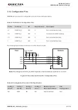
3.14. Configuration Pins
RM505Q-AE provides four configuration pins, which are defined as below.
Table 21: Definition of Configuration Pins
The following figure shows a reference circuit for these four pins.
Host
Module
CONFIG_0
CONFIG_1
CONFIG_2
CONFIG_3
GPIO
GPIO
GPIO
GPIO
21
69
75
1
VCC_IO_HOST
R1
10K
R2
10K
R3
10K
R4
10K
NM-0
Ω
NM-0
Ω
NM-0
Ω
0
Ω
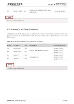
Note:
The voltage level of VCC_IO_HOST depends on the host side and could be 1.8 V or 3.3 V.
Figure 26: Recommended Circuit for Configuration Pins
Table 22: Configuration Pins List of M.2 Specification
Pin No.
Pin Name
I/O
Power Domain
Description
21
CONFIG_0
DO
0
Not connected internally
69
CONFIG_1
DO
0
Connected to GND internally
75
CONFIG_2
DO
0
Not connected internally
1
CONFIG_3
DO
0
Not connected internally
Config_0
(Pin 21)
Config_1
(Pin 69)
Config_2
(Pin 75)
Config_3
(Pin 1)
Module Type and
Main Host Interface
Port
Configuration
NC
GND
NC
NC
Quectel defined
N/A

