


M20 Hardware Design
4 Antenna interface
The RF interface has an impedance of 50
Ω
. To suit the physical design of individual application
M20 offers two alternatives:
z
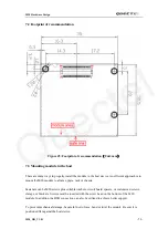
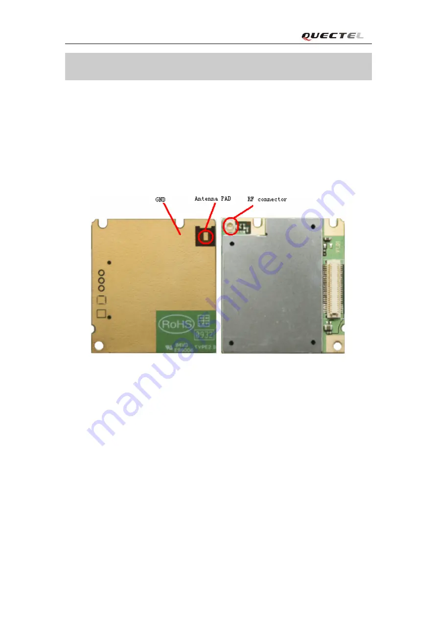
Recommended approach: antenna connector at the component side of the PCB (top view on
M20).
z
Antenna pad and ground plane placed at the bottom side.
When an antenna is connected to the pad, the Hirose connector must be left empty and vice versa.
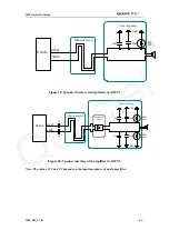
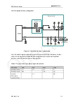
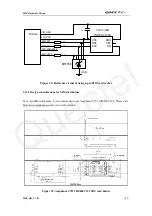
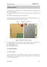
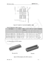
The antenna PAD and RF connector are shown in Figure 42:
Figure 42
: Antenna PAD and RF connector
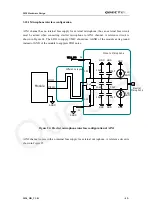
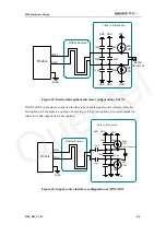
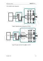
To minimize the loss on the RF cable, RF cable should be chosen very carefully. It is
recommended that the insertion loss should try to meet the following requirements:
z
GSM850/GSM900<1dB
z
DCS1800/PCS1900<1.5dB
4.1 Antenna installation
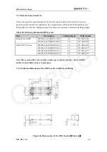
4.1.1 Antenna connector
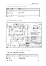
The module adopts Hirose’s U.FL-R-SMT RF connector. Customer is recommended to use
Hirose’s U.FL-LP as the matching connector at the application side. The specification of
U.FL-R-SMT is listed in Table 27:
M20_HD_V1.01
- 62 -
Quectel


