background image


                                                                                                                          Wi-Fi&Bluetooth  Module  Series


FC800L_Hardware_Design                                                                                                                          44 / 50 


5


Mechanical Information 


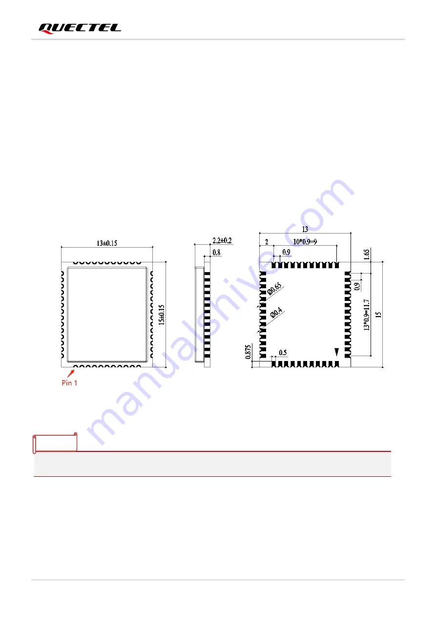
This chapter describes the mechanical dimensions of FC800L. All dimensions are measured in millimeter 

(mm), and the dimensional tolerances are ±0.2 mm unless otherwise specified.   


5.1. Mechanical Dimensions 


Figure 16: Top and Side Dimensions (Top and Side View) 


The package warpage level of the module conforms to

 JEITA ED-7306 

standard. 


NOTE 

Содержание FC800L

Страница 1: ...FC800L Hardware Design Wi Fi Bluetooth Module Series Version 1 0 3 Date 2022 08 22 Status Preliminary ...

Страница 2: ...cially reasonable efforts to provide the best possible experience you hereby acknowledge and agree that this document and related services hereunder are provided to you on an as available basis We may revise or restate this document from time to time at our sole discretion without any prior notice to you Copyright Our and third party products hereunder may contain copyrighted material Such copyrig...

Страница 3: ...iers or customer designated servers Quectel strictly abiding by the relevant laws and regulations shall retain use disclose or otherwise process relevant data for the purpose of performing the service only or as permitted by applicable laws Before data interaction with third parties please be informed of their privacy and data security policy Disclaimer a We acknowledge no liability for any injury...

Страница 4: ...se interference on sensitive medical equipment so please be aware of the restrictions on the use of wireless devices when in hospitals clinics or other healthcare facilities Cellular terminals or mobiles operating over radio signal and cellular network cannot be guaranteed to connect in certain conditions such as when the mobile bill is unpaid or the U SIM card is invalid When emergent help is nee...

Страница 5: ...022 04 13 Arrow HUANG Preliminary 1 Updated operating temperature 1 0 2 2022 04 27 Arrow HUANG Preliminary 1 Updated operating mode Table 2 Table 29 1 0 3 2022 08 22 Arrow HUANG Preliminary 1 Update RF characteristics 2 Update power consumption 3 Updated WLAN_WAKE pin description and added SDIO interrupt description 4 Updated evaluation board description and module weights 5 Added chapter 3 8 RF A...

Страница 6: ...N_WAKE 24 3 5 2 SDIO Interface 24 3 6 Bluetooth Application Interface 25 3 6 1 BT_EN 26 3 6 2 UART Interface 26 3 6 3 BT_WAKE_HOST and HOST_WAKE_BT 27 3 6 4 PCM Interface 27 3 7 Other Interfaces 28 3 7 1 RTC_CLK 28 3 7 2 CHIP_EN 29 3 8 RF Antenna Interfaces 30 3 8 1 Operating Frequency 30 3 8 2 Pin Definition of RF Antenna Interface 30 3 8 3 Reference Design of RF Antenna Interfaces 30 3 8 4 Refer...

Страница 7: ...Performance 42 4 6 Electrostatic Discharge 43 5 Mechanical Information 44 5 1 Mechanical Dimensions 44 5 2 Recommended Footprint 45 5 3 Top and Bottom Views 46 6 Storage Manufacturing and Packaging 47 6 1 Storage Conditions 47 6 2 Manufacturing and Soldering 48 6 3 Packaging Specifications 50 6 3 1 Carrier Tape 50 6 3 2 Plastic Reel 51 6 3 3 Packaging Process 52 7 Appendix References 53 ...

Страница 8: ...T_WAKEUP_BT 27 Table 11 Pin Definition of PCM Interface 28 Table 12 Pin Definition of RTC_CLK 28 Table 13 Pin Definition of CHIP_EN 29 Table 14 Conducted RF Output Power at 2 4 GHz 40 Table 15 Conducted RF Output Power at 5 GHz 40 Table 16 Conducted RF Receiving Sensitivity at 2 4 GHz 41 Table 17 Conducted RF Receiving Sensitivity at 5 GHz 41 Table 18 Electrostatics Discharge Characteristics 25 C ...

Страница 9: ... Coplanar Waveguide Design on a 2 layer PCB 32 Figure 12 Coplanar Waveguide Design on a 4 layer PCB Layer 3 as Reference Ground 32 Figure 13 Coplanar Waveguide Design on a 4 layer PCB Layer 4 as Reference Ground 33 Figure 14 Dimensions of the U FL R SMT Connector Unit mm 34 Figure 15 Mechanicals of UF L LP Connectors Unit mm 35 Figure 16 Space Factor of Mated Connector Unit mm 35 Figure 17 Top and...

Страница 10: ... complies with FCC radiation exposure limits set forth for an uncontrolled environment In order to avoid the possibility of exceeding the FCC radio frequency exposure limits human proximity to the antenna shall not be less than 20cm 8 inches during normal operation This transmitter must not be co located or operating in conjunction with any other antenna or transmitter Any changes or modifications...

Страница 11: ...antennas and or higher gain antennas may require additional authorization for operation 4 The max allowed antenna gain is WIFI 2 4G BT 0 52dBi WIFI 5G 0 66 dBi for external antenna In the event that these conditions cannot be met for example certain laptop configurations or co location with another transmitter then the FCC authorization is no longer considered valid and the FCC ID IC ID cannot be ...

Страница 12: ...f module 1 L antenne doit ê tre installé e de telle sorte qu une distance de 20 cm est respecté e entre l antenne et les utilisateurs et 2 Le module é metteur peut ne pas ê tre coï mplantéavec un autre é metteur ou antenne Tant que les 2 conditions ci dessus sont remplies des essais supplé mentaires sur l é metteur ne seront pas né cessaires Toutefois l inté grateur OEM est toujours responsable de...

Страница 13: ...ion To the End User The OEM integrator has to be aware not to provide information to the end user regarding how to install or remove this RF module in the user s manual of the end product which integrates this module The end user manual shall include all required regulatory information warning as show in this manual Manuel d information à l utilisateur final L intégrateur OEM doit être conscient d...

Страница 14: ...rôle ou de signalisation ou l utilisation de codes répétitifs lorsque cela est requis par la technologie Avertissement i Le dispositif utilisé dans la bande 5150 5250 MHz est réservé à une utilisation en intérieur afin de réduire le risque de brouillage préjudiciable aux systèmes mobiles par satellite dans le même canal ii lorsqu il y a lieu les types d antennes s il y en a plusieurs les numéros d...

Страница 15: ...ction 6 2 2 3 shall be clearly indicated 1 1 Special Mark Table 1 Special Mark Mark Definition Unless otherwise specified when an asterisk is used after a function feature interface pin name AT command or argument it indicates that the function feature interface pin AT command or argument is under development and currently not supported and the asterisk after a model indicates that the sample of s...

Страница 16: ...CM interface for Bluetooth FC800L can provide WLAN and Bluetooth functions 2 2 Key Features The following table describes the key features of FC800L Table 2 Key Features Features Details Power Supply VBAT power supply Supply voltage range 2 97 3 63 V Typical supply voltage 3 3 V VDDIO power supply Supply voltage range 1 62 1 98 V Typical supply voltage 1 8 V Operating Frequency 2 4 GHz WLAN 2 400 ...

Страница 17: ... 3 dBm 802 11ac VHT20 MCS8 13 3 dBm 802 11ac VHT40 MCS9 12 3 dBm 802 11ac VHT80 MCS9 11 3 dBm Operation Mode STA Modulation CCK BPSK QPSK 16QAM 64QAM 256QAM WLAN Application Interface SDIO 3 0 Bluetooth Application Interface UART and PCM RF Antenna Interfaces ANT_WIFI ANT_BT Physical Characteristics Size 13 0 15 mm 15 0 15 mm 2 2 0 2 mm Package LCC Weight about 0 8g Temperature Range Operating tem...

Страница 18: ...Wi Fi Bluetooth Module Series FC800L_Hardware_Design 17 50 2 3 EVB Quectel supplies an evaluation board FC800L M 2 with accessories to control or test the module ...

Страница 19: ...s 3 1 General Description FC800L is equipped with 50 LCC pins The subsequent chapters will provide a detailed introduction to the following interfaces and pins of the module Power supply WLAN application interface Bluetooth application interface RF antenna interfaces Other interfaces ...

Страница 20: ... 44 41 40 39 38 37 14 13 12 16 17 19 20 18 21 22 23 24 25 GND GND GND GND RESERVED GND RESERVED RESERVED 33 31 30 32 29 28 27 26 35 34 36 RESERVED PCM_SYNC PCM_DIN PCM_DOUT RTC_CLK PCM_CLK VBAT GND VDDIO RESERVED RESERVED RESERVED GND BT_EN BT_TXD BT_RXD BT_RTS BT_CTS RESERVED RESERVED RESERVED GND RESERVED HOST_WAKE_BT BT_WAKE_HOST FC800L GND Power WLAN RESERVED Bluetooth RF Other signals 15 Figu...

Страница 21: ... Input PO Power Output Power Supply Pin Name Pin No I O Description Comment VBAT 36 PI Power supply for the module It must be provided with sufficient current up to 1 2 A VDDIO 34 PI Power supply for module s I O pins VDDIO only support 1 8 V GND 1 3 8 10 11 23 32 39 47 WLAN Application Interface Pin Name Pin No I O Description Comment WLAN_WAKE 16 DO Wake up the host by WLAN and SDIO interrupt fu...

Страница 22: ... sync VDDIO power domain PCM_DIN 28 DI PCM data input PCM_DOUT 29 DO PCM data output PCM_CLK 30 DI PCM clock BT_EN 38 DI Bluetooth enable control Active high VDDIO power domain BT_TXD 40 DO Bluetooth UART transmit VDDIO power domain BT_RXD 41 DI Bluetooth UART receive BT_RTS 42 DO Bluetooth UART request to send BT_CTS 43 DI Bluetooth UART clear to send HOST_WAKE_BT 49 DI Host wakes up Bluetooth BT...

Страница 23: ...68 kHz clock input VDDIO power domain CHIP_EN 15 DI Module enable pin Pull up to VDDIO internally through a 4 7 kΩ resistor high level by default VDDIO power domain RF Antenna Interfaces Pin Name Pin No I O Description Comment ANT_BT 2 AIO Bluetooth antenna interface 50 Ω impedance ANT_WIFI 9 AIO Wi Fi antenna interface RESERVED Interfaces Pin Name Pin No I O Description Comment RESERVED 12 14 24 ...

Страница 24: ...the same time as VDDIO VDDIO should not be present first or be held high before VBAT is high 2 RTC_CLK must held stable before CHIP_EN held high 3 5 WLAN Application Interface HOST FC800L SDIO3 0 GPIO_1 WLAN_WAKE SDIO3 0 Figure 3 WLAN Application Interface Connection The following figure shows the WLAN application interface connection between FC800L and the host NOTE ...

Страница 25: ... Definition of SDIO Interface The following figure shows the SDIO interface connection between FC800L and host Pin Name Pin No I O Description Comment WLAN_WAKE 16 DO Wake up the host by WLAN and SDIO interrupt function GPIO_1 connected to WLAN_WAKE must be interruptible Pin Name Pin No I O Description Comment SDIO_CMD 17 DIO SDIO command VDDIO power domain SDIO_CLK 18 DI SDIO clock SDIO_DATA3 19 ...

Страница 26: ...such as radio frequency analog signals clocks and DC DC noise signals The distance between SDIO signals and other signals must be greater than 2 times the trace width and the busload capacitance must be less than 15 pF SDIO signal traces need to be treated with equal length the distance between the traces is less than 1 mm According to the transmission rate the trace length has the following requi...

Страница 27: ...n BT_EN is at high level Table 8 Pin Definition of BT_EN 3 6 2 UART Interface FC800L supports an HCI UART as defined in Bluetooth Core Specification Version 5 0 The UART supports hardware flow control and it is used for data transmission with host It supports up to 4 0 Mbps baud rates The following table shows the pin definition of UART interface Table 9 Pin Definition of UART Interface GPIO_2 con...

Страница 28: ...RT_CTS UART_RTS Host Figure 6 Reference Design for UART Interface Connection 3 6 3 BT_WAKE_HOST and HOST_WAKE_BT Table 10 Pin Definition of BT_WAKEUP_HOST and HOST_WAKEUP_BT Pin Name Pin No I O Description Comment HOST_WAKE_BT 49 DI Host wakes up Bluetooth VDDIO power domain BT_WAKE_HOST 50 DO Bluetooth wakes up host 3 6 4 PCM Interface PCM interface is used for audio over Bluetooth phone The foll...

Страница 29: ...gure 7 PCM Interface Connection 3 7 Other Interfaces 3 7 1 RTC_CLK The RTC_CLK 32 768 kHz is used for internal PMU reference clock Table 12 Pin Definition of RTC_CLK Pin Name Pin No I O Description Comment RTC_CLK 31 DI External 32 768 kHz clock input Pin Name Pin No I O Description Comment PCM_SYNC 27 DI PCM data frame sync VDDIO power domain PCM_DIN 28 DI PCM data input PCM_DOUT 29 DO PCM data o...

Страница 30: ...e Series FC800L_Hardware_Design 29 50 3 7 2 CHIP_EN The module is enabled by CHIP_EN Table 13 Pin Definition of CHIP_EN Pin Name Pin No I O Description Comment CHIP_EN 15 DI Module enable pin Active high VDDIO power domain ...

Страница 31: ... No I O Description Comment ANT_BT 2 AIO Bluetooth antenna interface 50 Ω impedance ANT_WIFI 9 AIO Wi Fi antenna interface 0 50 Ω impedance FC800L module provides an RF antenna pin for Wi Fi Bluetooth antenna connection The RF trace in host PCB connected to the module s RF antenna pin should be microstrip line or other types of RF trace with characteristic impendence close to 50 Ω FC800L module co...

Страница 32: ...Wi Fi Bluetooth Module Series FC800L_Hardware_Design 31 50 Figure 8 Reference Circuit for RF Antenna Interfaces ...

Страница 33: ...he characteristic impedance of all RF traces should be controlled to 50 Ω The impedance of the RF traces is usually determined by the trace width W the materials dielectric constant the height from the reference ground to the signal layer H and the spacing between RF traces and grounds S Microstrip or coplanar waveguide is typically used in RF layout to control characteristic impedance The followi...

Страница 34: ...curved ones The recommended trace angle is 135 There should be clearance under the signal pin of the antenna connector or solder joint The reference ground of RF traces should be complete Meanwhile adding some ground vias around RF traces and the reference ground could help to improve RF performance The distance between the ground vias and RF traces should be no less than two times the width of RF...

Страница 35: ... 1 Max Input Power W 50 Input Impedance Ω 50 Polarization Type Vertical 3 8 6 Recommended RF Connector for Antenna Installation Figure 13 Dimensions of the U FL R SMT Connector Unit mm U FL LP serial connectors listed in the following figure can be used to match the U FL R SMT If RF connector is used for antenna connection it is recommended to use U FL R SMT connector provided by Hirose ...

Страница 36: ...ardware_Design 35 50 Figure 14 Mechanicals of UF L LP Connectors Unit mm The following figure describes the space factor of mated connector Figure 15 Space Factor of Mated Connector Unit mm For more details please visit http www hirose com ...

Страница 37: ...ics Power consumption RF performance ESD protection Operating and storage temperature 4 2 Electrical Characteristics Table 5 Absolute Maximum Ratings This chapter mainly introduces the electrical characteristics and radio frequency characteristics of FC800L the specific content is as follows Parameter Min Max Unit VBAT 0 5 3 63 V VDDIO 0 5 3 63 V Digital I O Input Voltage 0 5 3 63 V ...

Страница 38: ...ons of FC800L module Parameter Min Typ Max Unit VBAT 2 97 3 3 3 63 V VDDIO 1 62 1 8 1 98 V The following table shows the general DC electrical characteristics over recommended operating conditions unless otherwise specified Symbol Parameter Min Max Unit VIH High level Input Voltage 0 65 VDDIO VDDIO 0 3 V VIL Low level Input Voltage 0 3 0 35 VDDIO V VOH High level Output Voltage VDDIO 0 2 VDDIO 0 3...

Страница 39: ...66 50 0 04 mA TX 2 4 GHz 54 Mbps 165 50 0 04 mA 802 11n TX 2 4 GHz HT20 MCS0 265 50 0 04 mA TX 2 4 GHz HT20 MCS7 158 00 0 05 mA TX 2 4 GHz HT40 MCS0 261 00 0 04 mA TX 2 4 GHz HT40 MCS7 161 00 0 02 mA TX 5 GHz HT20 MCS0 441 50 0 04 mA TX 5 GHz HT20 MCS7 250 00 0 05 mA TX 5 GHz HT40 MCS0 443 50 0 04 mA TX 5 GHz HT40 MCS7 277 50 0 01 mA 802 11a TX 5 GHz 6 Mbps 443 00 0 04 mA TX 5 GHz 54 Mbps 264 50 0...

Страница 40: ...Wi Fi Bluetooth Module Series FC800L_Hardware_Design 39 50 TX 5 GHz VHT80 MCS0 431 50 0 04 mA TX 5 GHz VHT80 MCS9 167 50 0 02 mA ...

Страница 41: ...13 15 dBm 802 11n HT20 MCS0 15 17 dBm 802 11n HT20 MCS7 12 14 dBm 802 11n HT40 MCS0 14 16 dBm 802 11n HT40 MCS7 12 14 dBm Table 15 Conducted RF Output Power at 5 GHz The following tables summarize the transmitting and receiving performances of FC800L Standard Min Typ Unit 802 11a 6 Mbps 14 17 dBm 802 11a 54 Mbps 12 15 dBm 802 11n HT20 MCS0 14 17 dBm 802 11n HT20 MCS7 11 14 dBm 802 11n HT40 MCS0 13...

Страница 42: ...S0 11 14 dBm 802 11ac VHT80 MCS9 8 11 dBm Standard Receiving Sensitivity Typ 802 11b 1 Mbps 95 5 dBm 802 11b 11 Mbps 87 0 dBm 802 11g 6 Mbps 93 0 dBm 802 11g 54 Mbps 76 0 dBm 802 11n HT20 MCS0 92 5 dBm 802 11n HT20 MCS7 74 5 dBm 802 11n HT40 MCS0 89 0 dBm 802 11n HT40 MCS7 70 5 dBm Standard Receiving Sensitivity Typ 802 11a 6 Mbps 94 0 dBm 802 11a 54 Mbps 75 0 dBm 802 11n HT20 MCS0 93 0 dBm 802 11...

Страница 43: ...module 802 11ac VHT20 MCS0 92 5 dBm 802 11ac VHT20 MCS8 69 5 dBm 802 11ac VHT40 MCS0 89 0 dBm 802 11ac VHT40 MCS9 64 5 dBm 802 11ac VHT80 MCS0 84 0 dBm 802 11ac VHT80 MCS9 59 0 dBm Standard Transmitting Power Receiving Sensitivity Unit BR 6 8 90 0 dBm EDR π 4 DQPSK 5 1 90 5 dBm EDR 8 DPSK 5 1 85 5 dBm BLE 1M 6 7 98 5 dBm BLE 2M 6 7 96 0 dBm S 2 6 7 100 5 dBm S 8 6 7 103 5 dBm ...

Страница 44: ...s is imperative For example wear anti static gloves during the development production assembly and testing of the module add ESD protection components to the ESD sensitive interfaces and points in the product design Table 18 Electrostatics Discharge Characteristics 25 C 45 Relative Humidity Unit kV Tested Interfaces Contact Discharge Air Discharge Unit VBAT GND 2 12 kV ANT_BT ANT_WIFI 5 10 kV Othe...

Страница 45: ... the mechanical dimensions of FC800L All dimensions are measured in millimeter mm and the dimensional tolerances are 0 2 mm unless otherwise specified 5 1 Mechanical Dimensions Figure 16 Top and Side Dimensions Top and Side View The package warpage level of the module conforms to JEITA ED 7306 standard NOTE ...

Страница 46: ...Hardware_Design 45 50 5 2 Recommended Footprint Figure 17 Recommended Footprint Top View 1 For easy maintenance of this module keep at least 3 mm between the module and other components on the motherboard 2 Keep all RESERVED pins open NOTE ...

Страница 47: ...gn 46 50 5 3 Top and Bottom Views Figure 18 Top and Bottom Views of the Module Images above are for illustration purpose only and may differ from the actual module For authentic appearance and label please refer to the module received from Quectel NOTE ...

Страница 48: ... than 10 e g a drying cabinet 4 The module should be pre baked to avoid blistering cracks and inner layer separation in PCB under the following circumstances The module is not stored in Recommended Storage Condition Violation of the third requirement above occurs Vacuum sealed packaging is broken or the packaging has been removed for over 24 hours Before module repairing 5 If needed the pre baking...

Страница 49: ...aste fill the stencil openings and then penetrate to the PCB Apply proper force on the squeegee to produce a clean stencil surface on a single pass To guarantee module soldering quality the thickness of stencil for the module is recommended to be 0 13 0 15 mm For more details see document 2 The peak reflow temperature should be 238 246 º C with 246 º C as the absolute maximum reflow temperature To...

Страница 50: ...that after 12 hours Neutral Salt Spray test the laser engraved label information on the shielding can is still clearly identifiable and the QR code is still readable although white rust may be found 3 If a conformal coating is necessary for the module do NOT use any coating material that may chemically react with the PCB or shielding cover and prevent the coating material from flowing into the mod...

Страница 51: ...ecifications The module adopts carrier tape packaging and details are as follow 6 3 1 Carrier Tape Dimension details are as follow Figure 20 Carrier Tape Dimension Drawing Table 20 Carrier Tape Dimension Table Unit mm W P T A0 B0 K0 K1 F E 32 20 0 4 13 4 15 4 2 7 5 4 14 2 1 75 ...

Страница 52: ...Wi Fi Bluetooth Module Series FC800L_Hardware_Design 51 50 6 3 2 Plastic Reel Figure 21 Plastic Reel Dimension Drawing Table 21 Plastic Reel Dimension Table Unit mm øD1 øD2 W 330 100 32 5 ...

Страница 53: ...hem then wind the heat sealed carrier tape to the plastic reel and use the protective tape for protection One plastic reel can load 500 modules Place the packaged plastic reel humidity indicator card and desiccant bag into a vacuum bag then vacuumize it Place the vacuum packed plastic reel into a pizza box Put 4 pizza boxes into 1 carton and seal it One carton can pack 2000 modules ...

Страница 54: ...condary_SMT_Application_Note Abbreviation Description BPSK Binary Phase Shift Keying BT Bluetooth CCK Complementary Code Keying CTS Clear to Send GND Ground HCI Host Controller Interface IEEE Institute of Electrical and Electronics Engineers IIL Input Leakage Current I O Input Output LNA Low Noise Amplifier LTE Long Term Evolution Mbps Megabits per second MCS Modulation and Coding Scheme PA Power ...

Страница 55: ...adrature Amplitude Modulation QPSK Quadrature Phase Shift Keying RF Radio Frequency RoHS Restriction of Hazardous Substances RTS Request to Send RX Receive TBD To Be Determined TX Transmit UART Universal Asynchronous Receiver Transmitter VHT Very High Throughput Wi Fi Wireless Fidelity WLAN Wireless Local Area Network ...

Отзывы: