

LTE Standard Module Series
EG25-GL_Hardware_Design 65 / 96
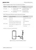
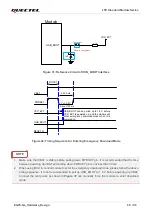
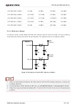
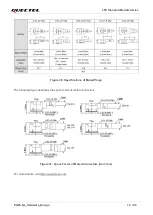
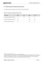
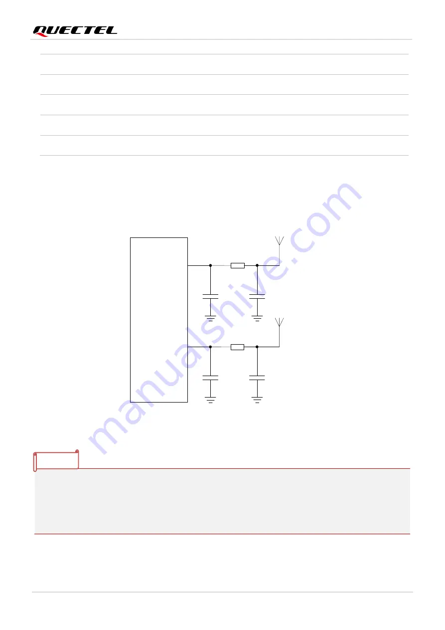
5.1.4 Reference Design
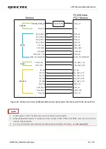
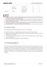
A reference design of ANT_MAIN and ANT_DIV antenna pads is shown as below.
A π-type matching
circuit should be reserved for better RF performance. The capacitors are not mounted by default.
ANT_MAIN
R1 0R
C1
Module
Main
Antenna
NM
C2
NM
R2 0R
C3
Diversity
Antenna
NM
C4
NM
ANT_DIV
Figure 33: Reference Circuit of RF Antenna Interface
1. Keep a proper distance between the main antenna and the Rx-diversity antenna to improve the
receiving sensitivity.
2. For the operation of ANT_MAIN and ANT_DIV, see
AT+QCFG="divctl"
in
document [3]
for details.
3. Place the
π-type matching components (R1, C1 and C2; R2, C3 and C4) as close to the antenna as
possible.
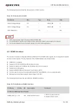
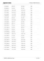
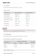
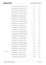
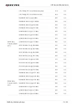
LTE-TDD B38 (10 MHz)
-97 dBm
-97 dBm
-100 dBm
-96.3 dBm
LTE-TDD B39 (10 MHz)
-97.5 dBm
-97.5 dBm
-100 dBm
-96.3 dBm
LTE-TDD B40 (10 MHz)
-97.3 dBm
-97.5 dBm
-100.5dBm
-96.3 dBm
LTE-TDD B41 (10 MHz)
-96.3 dBm
-97 dBm
-99.5 dBm
-94.3 dBm
LTE-FDD B66 (10 MHz)
-96 dBm
-96 dBm
-99.5 dBm
-94.8 dBm
NOTE
Содержание EG25-GL
Страница 1: ...EG25 GL Hardware Design LTE Standard Module Series Version 1 0 0 Date 2022 09 09 Status Preliminary ...
Страница 8: ...LTE Standard Module Series EG25 GL_Hardware_Design 7 96 9 Appendix References 92 ...
Страница 10: ...LTE Standard Module Series EG25 GL_Hardware_Design 9 96 Table 42 Terms and Abbreviations 92 ...


