


LTE Standard Module Series
EG25-GL_Hardware_Design 43 / 96
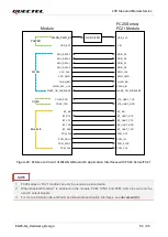
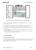
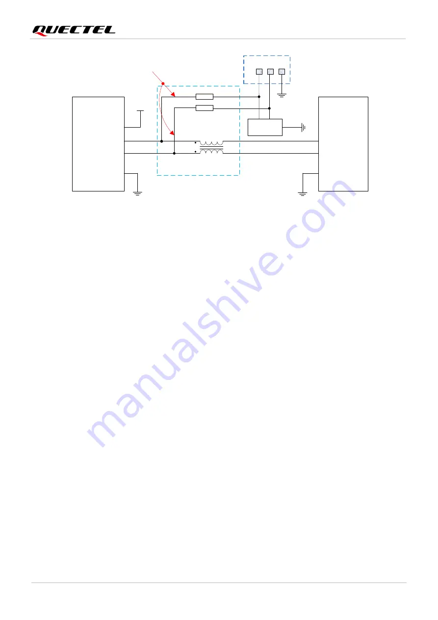
USB_DP
USB_DM
GND
USB_DP
USB_DM
GND
L1
Close to Module
R3
R4
Test Points
ESD Array
NM_0R
NM_0R
Minimize these stubs
Module
MCU
USB_VBUS
VDD
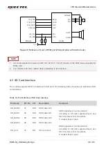
Figure 19: Reference Circuit of USB Interface
A common-mode choke L1 is recommended to be added in series between the module and your MCU to
suppress EMI spurious transmission. Meanwhile, the 0
Ω resistors (R3 and R4) should be added in series
between the module and the test points so as to facilitate debugging, and the resistors are not mounted
by default. To ensure the integrity of USB data trace signal, L1/R3/R4 component must be placed close to
the module, and also these resistors should be placed close to each other. The extra stubs of trace must
be as short as possible.
The following principles should be complied with when design the USB interface, to meet USB 2.0
specification.
⚫
It is important to route the USB signal traces as differential pairs with total grounding. The impedance
of USB differential trace is 90
Ω.
⚫
Do not route signal traces under crystals, oscillators, magnetic devices and RF signal traces. It is
important to route the USB differential traces in inner-layer, and surround the traces with ground on
that layer and with ground planes above and below.
⚫
Junction capacitance of the ESD protection component might cause influences on USB data traces,
so pay attention to the selection of the component. Typically, the stray capacitance should be less
than 2 pF.
⚫
Keep the ESD protection components to the USB connector as close as possible.
4.3 UART Interfaces
The module provides two UART interfaces: the main UART interface and the debug UART interface. The
following shows their features.
⚫
The main UART interface supports 4800, 9600, 19200, 38400, 57600, 115200, 230400, 460800 and
Содержание EG25-GL
Страница 1: ...EG25 GL Hardware Design LTE Standard Module Series Version 1 0 0 Date 2022 09 09 Status Preliminary ...
Страница 8: ...LTE Standard Module Series EG25 GL_Hardware_Design 7 96 9 Appendix References 92 ...
Страница 10: ...LTE Standard Module Series EG25 GL_Hardware_Design 9 96 Table 42 Terms and Abbreviations 92 ...


