background image


LTE Standard Module Series


EG25-GL_Hardware_Design                                                                                                                    44  / 96 


921600 bps baud rates, and the default is 115200 bps. It also supports RTS and CTS hardware flow 

control, and can be used for data transmission and AT command communication. 


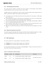
The  debug  UART  interface  supports  115200  bps  baud  rate.  It  is  used  for  Linux  console  and  log 

output.   


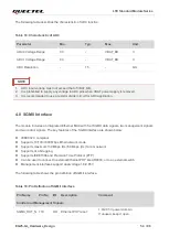
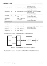
The following tables show the pin definition of the UART interfaces. 


Table 12: Pin Definition of Main UART Interface 


Table 13: Pin Definition of Debug UART Interface 


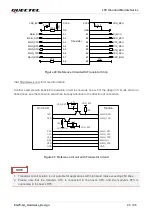
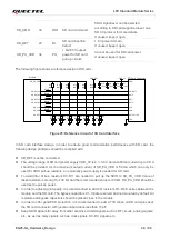
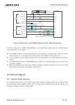
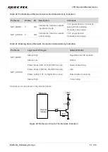
The  module  provides  1.8  V  UART  interfaces.  A  level  translator  should  be  used  if  your  application  is 

equipped with a 3.3 V UART interface. A level translator TXS0108EPWR provided by Texas Instruments 

is recommended. The following figure shows a reference design. 

Pin Name   

Pin No. 

I/O 

Description   

Comment 

MAIN_RI 

62 

DO 

Main UART ring indication 

1.8 V power domain. 

If unused, keep it open. 

MAIN_DCD 

63 

DO 

Main UART data carrier detect 

MAIN_CTS 

64 

DO 

DTE clear to send signal from DCE 

Connect to DTE

’s CTS

1.8 V power domain. 

If unused, keep it open. 

MAIN_RTS 

65 

DI 

DTE request to send signal to DCE 

Connect to DTE's RTS. 

1.8 V power domain. 

If unused, keep it open. 

MAIN_DTR 

66 

DI 

Main UART data terminal ready 

1.8 V power domain. 

Pulled up by default.   

The pin can wake up the module 

in the low level. 

If unused, keep it open. 

MAIN_TXD 

67 

DO 

Main UART transmit 

1.8 V power domain. 

If unused, keep it open. 

MAIN_RXD 

68 

DI 

Main UART receive 

Pin Name   

Pin No. 

I/O 

Description   

Comment 

DBG_TXD 

12 

DO 

Debug UART transmit 

1.8 V power domain. 

If unused, keep it open. 

DBG_RXD 

11 

DI 

Debug UART receive 

Содержание EG25-GL

Страница 1: ...EG25 GL Hardware Design LTE Standard Module Series Version 1 0 0 Date 2022 09 09 Status Preliminary ...

Страница 2: ... we employ commercially reasonable efforts to provide the best possible experience you hereby acknowledge and agree that this document and related services hereunder are provided to you on an as available basis We may revise or restate this document from time to time at our sole discretion without any prior notice to you Use and Disclosure Restrictions License Agreements Documents and information ...

Страница 3: ... To implement module functionality certain device data are uploaded to Quectel s or third party s servers including carriers chipset suppliers or customer designated servers Quectel strictly abiding by the relevant laws and regulations shall retain use disclose or otherwise process relevant data for the purpose of performing the service only or as permitted by applicable laws Before data interacti...

Страница 4: ...nterference on sensitive medical equipment so please be aware of the restrictions on the use of wireless devices when in hospitals clinics or other healthcare facilities Cellular terminals or mobiles operating over radio signal and cellular network cannot be guaranteed to connect in certain conditions such as when the mobile bill is unpaid or the U SIM card is invalid When emergency help is needed...

Страница 5: ...d Module Series EG25 GL_Hardware_Design 4 96 About the Document Revision History Version Date Author Description 2022 09 09 Ethan FANG Joe MA Creation of the document 1 0 0 2022 09 09 Ethan FANG Joe MA Preliminary ...

Страница 6: ...B Application Scenario 29 3 2 2 1 USB Application with USB Remote Wakeup Function 29 3 2 2 2 USB Application with USB Suspend Resume and MAIN_RI Function 30 3 2 2 3 USB Application without USB Suspend Function 31 3 2 3 Airplane Mode 31 3 3 Power Supply 32 3 3 1 Power Supply Pins 32 3 3 2 Voltage Stability Requirements 33 3 3 3 Reference Design for Power Supply 34 3 3 4 Power Supply Voltage Monitor...

Страница 7: ...ntenna Interface Frequency Bands 66 5 2 2 GNSS Performance 67 5 2 3 Reference Design 68 5 3 RF Routing Guidelines 68 5 4 Antenna Design Requirements 70 5 5 RF Connector Recommendation 71 6 Electrical Characteristics and Reliability 73 6 1 Absolute Maximum Ratings 73 6 2 Power Supply Ratings 74 6 3 Power Consumption 74 6 4 ESD Protection 79 6 5 Operating and Storage Temperatures 80 7 Mechanical Inf...

Страница 8: ...LTE Standard Module Series EG25 GL_Hardware_Design 7 96 9 Appendix References 92 ...

Страница 9: ... ADC 54 Table 19 Pin Definition of SGMII Interface 54 Table 20 Pin Definition of Network Connection Status Activity Indication 57 Table 21 Working State of Network Connection Status Activity Indication 57 Table 22 Pin Definition of STATUS 58 Table 23 Behaviors of MAIN_RI 59 Table 24 Pin Definition of USB_BOOT Interface 59 Table 25 Pin Definition of Antenna Antennas 61 Table 26 Frequency Bands 61 T...

Страница 10: ...LTE Standard Module Series EG25 GL_Hardware_Design 9 96 Table 42 Terms and Abbreviations 92 ...

Страница 11: ... Circuit with Translator Chip 45 Figure 21 Reference Circuit with Transistor Circuit 45 Figure 22 Primary Mode Timing 46 Figure 23 Auxiliary Mode Timing 47 Figure 24 Reference Circuit of PCM and I2C Application with Audio Codec 48 Figure 25 Reference Circuit of SD Card Interface 49 Figure 26 Reference Circuit of WLAN Bluetooth Application Interfaces with FC20 Series FC21 52 Figure 27 Simplified Bl...

Страница 12: ...om View 82 Figure 44 Recommended Footprint Top View 83 Figure 45 Recommended Compatible Footprint Top View 84 Figure 46 Top and Bottom Views of the Module 85 Figure 47 Recommended Reflow Soldering Thermal Profile 87 Figure 48 Carrier Tape Dimension Drawing 89 Figure 49 Plastic Reel Dimension Drawing 89 Figure 50 Packaging Process 91 ...

Страница 13: ... to design and set up mobile applications with the module 1 1 Special Marks Table 1 Special Marks Mark Definition Unless otherwise specified when an asterisk is used after a function feature interface pin name AT command or argument it indicates that the function feature interface pin AT command or argument is under development and currently not supported and the asterisk after a model indicates t...

Страница 14: ...meet most requirements for M2M applications such as automation smart metering tracking system security router wireless POS mobile computing device PDA phone tablet PC etc EG25 GL is an SMD type module which can be embedded into applications through its 144 LGA 1 pins 1 LGA form factor is used for EG25 GL module while LCC is recommended only in the compatible design with EC25 series EC21 series EC2...

Страница 15: ...ass 3 23 dBm 2 dB for LTE FDD bands Class 3 23 dBm 2 dB for LTE TDD bands LTE Features Supports up to non CA Cat 4 FDD and TDD Supports 1 4 3 5 10 15 20 MHz RF bandwidth Supports MIMO in DL direction LTE FDD Max 150 Mbps DL Max 50 Mbps UL LTE TDD Max 130 Mbps DL Max 30 Mbps UL UMTS Features Supports 3GPP Rel 8 DC HSDPA HSPA HSDPA HSUPA and WCDMA Supports QPSK 16QAM and 64QAM modulation DC HSDPA Ma...

Страница 16: ...erface Compliant with USB 2 0 specification slave only the data transfer rate can reach up to 480 Mbps Used for AT command communication data transmission GNSS NMEA sentence output software debugging firmware upgrade and voice over USB Supports USB serial drivers for Windows 7 8 8 1 10 11 Linux 2 6 5 18 Android 4 x 12 x etc UART Interfaces Main UART Used for AT command communication and data trans...

Страница 17: ...ed the specified tolerances of 3GPP When the temperature returns to the operating temperature range the module meets 3GPP specifications again Antenna Interfaces Main antenna interface ANT_MAIN Rx diversity antenna interface ANT_DIV GNSS antenna interface ANT_GNSS Physical Characteristics Size 29 0 0 2 mm 32 0 0 2 mm 2 4 0 2 mm Package LGA Weight approx 4 9 g Temperature Range Operating temperatur...

Страница 18: ...nal parts Power management Baseband DDR2 NAND flash Radio frequency Peripheral interfaces ANT_MAIN ANT_DIV ANT_GNSS VBAT_BB VBAT_RF PWRKEY ADCs VDD_EXT USB U SIM PCM UARTs I2C RESET_N STATUS GPIOs Control IQ Control Tx PRx DRx WLAN SD Bluetooth SGMII PMU 19 2M XO Transceiver NAND DDR2 SDRAM Baseband APT SAW SAW SAW Switch Duplex PAM PA LNA Figure 1 Functional Diagram ...

Страница 19: ... GND RESERVED GND GND ANT_MAIN GND ANT_GNSS GND ADC1 RESERVED I2C_SDA I2C_SCL ADC0 GND GND GND 73 74 75 76 77 78 79 80 81 82 83 84 100 101 102 106 107 111 112 103 104 109 105 110 89 94 98 88 93 97 86 91 96 85 90 95 99 87 92 108 113 RESERVED RESERVED 117 126 125 124 123 122 121 118 127 128 115 USB_BOOT RESERVED 116 140 137 136 135 134 133 132 131 130 129 114 SD_PU_VDD Power Pins Signal Pins GND Pin...

Страница 20: ...on FC20 series or FC21 module 7 Keep all RESERVED pins and unused pins unconnected 8 GND pin 85 112 should be connected to ground in the design RESERVED pin 73 84 should not be designed in schematic and PCB decal and these pins should be served as a keepout area 2 5 Pin Description The following tables show the pin definition of EG25 GL module DC characteristics include power domain and rate curre...

Страница 21: ...its If unused keep it open GND 8 9 19 22 36 46 48 50 54 56 72 85 112 Turn On Off Pin Name Pin No I O Description DC Characteristics Comment PWRKEY 21 DI Turn on off the module The output voltage is 0 8 V because of the diode drop in the chipset RESET_N 20 DI Reset the module VIHmax 2 1 V VIHmin 1 3 V VILmax 0 5 V 1 8 V power domain If unused keep it open Indication Signals Pin Name Pin No I O Desc...

Страница 22: ...ifferential data U SIM Interface Pin Name Pin No I O Description DC Characteristics Comment USIM_GND 10 Specified ground for U SIM USIM_VDD 14 PO U SIM card power supply IOmax 50 mA Low voltage Vmax 1 9 V Vmin 1 7 V High voltage Vmax 3 05 V Vmin 2 7 V Either 1 8 V or 3 0 V is supported by the module automatically USIM_DATA 15 DIO U SIM card data USIM_VDD USIM_CLK 16 DO U SIM card clock USIM_VDD US...

Страница 23: ...fault The pin can wake up the module in the low level If unused keep it open MAIN_TXD 67 DO Main UART transmit VDD_EXT 1 8 V power domain If unused keep it open MAIN_RXD 68 DI Main UART receive VDD_EXT Debug UART Interface Pin Name Pin No I O Description DC Characteristics Comment DBG_TXD 12 DO Debug UART transmit VDD_EXT 1 8 V power domain If unused keep it open DBG_RXD 11 DI Debug UART receive V...

Страница 24: ...T I2C Interface Pin Name Pin No I O Description DC Characteristics Comment I2C_SCL 41 OD I2C serial clock for external codec VDD_EXT An external pull up to 1 8 V is required If unused keep it open I2C_SDA 42 OD I2C serial data for external codec VDD_EXT SD Card Interface Pin Name Pin No I O Description DC Characteristics Comment SD_DATA0 31 DIO SDIO data bit 0 SD_PU_VDD SDIO signal level can be se...

Страница 25: ...o I O Description DC Characteristics Comment WLAN_SLP_ CLK 118 DO WLAN sleep clock If unused keep it open WLAN_ PWR_EN 127 DO WLAN power supply enable control VDD_EXT 1 8 V power domain Active high If unused keep it open SDC_DATA0 132 DIO WLAN SDIO data bit 0 VDD_EXT 1 8 V power domain If unused keep it open SDC_DATA1 131 DIO WLAN SDIO data bit 1 VDD_EXT SDC_DATA2 130 DIO WLAN SDIO data bit 2 VDD_...

Страница 26: ...n BT_TXD 38 DO Bluetooth UART transmit VDD_EXT 1 8 V power domain If unused keep it open BT_RXD 39 DI Bluetooth UART receive VDD_EXT BT_CTS 40 DO DTE clear to send signal from DCE VDD_EXT Connect to DTE s CTS 1 8 V power domain Cannot be pulled up before startup If unused keep it open BT_EN 139 DO Bluetooth enable control VDD_EXT 1 8 V power domain If unused keep it open SGMII Interface Pin Name P...

Страница 27: ..._RX_M 126 AI SGMII receive SGMII_MDIO_ VDD 128 PO SGMII_MDIO pull up power supply IOmax 50 mA Configurable power source 1 8 2 85 V power domain If unused keep it open Antenna Interfaces Pin Name Pin No I O Description DC Characteristics Comment ANT_DIV 35 AI Diversity antenna interface 50 Ω impedance If unused keep it open ANT_MAIN 49 AIO Main antenna interface 50 Ω impedance ANT_GNSS 47 AI GNSS a...

Страница 28: ...rplane mode control VDD_EXT 1 8 V power domain Pull up by default At low voltage level module can enter into airplane mode If unused keep it open AP_READY 2 DI Application processor ready VDD_EXT 1 8 V power domain If unused keep it open USB_BOOT 115 DI Force the module into emergency download mode VDD_EXT 1 8 V power domain Cannot be pulled up before startup It is recommended to reserve test poin...

Страница 29: ...ata transfer rate Minimum Functionality Mode AT CFUN 0 can set the module to a minimum functionality mode without removing the power supply In this case both RF function and U SIM card will be invalid Airplane Mode AT CFUN 4 or W_DISABLE pin can set the module to enter airplane mode In this case RF function will be invalid Sleep Mode The current consumption of the module will be reduced to the min...

Страница 30: ...e host MAIN_DTR to low level will wake up the module When the module has a URC to report MAIN_RI will wake up the host See Chapter 4 9 3 for details about MAIN_RI behaviors AP_READY will detect the sleep state of the host It can be configured to high level or low level detection See document 3 for details about AT QCFG apready 3 2 2 USB Application Scenario 3 2 2 1 USB Application with USB Remote ...

Страница 31: ...cation with USB Suspend Resume and MAIN_RI Function If the host supports USB suspend and resume but does not support remote wakeup function MAIN_RI signal is needed to wake up the host There are three preconditions to set the module to sleep mode Execute AT QSCLK 1 to enable the sleep mode Ensure the MAIN_DTR is held at high level or keep it open The host s USB bus which is connected with the modu...

Страница 32: ...onnect USB_VBUS The following figure shows the connection between the module and the host USB_VBUS USB_DP USB_DM AP_READY VDD USB_DP USB_DM GPIO Module Host MAIN_RI EINT Power Switch GPIO GND GND Figure 6 Sleep Mode Application without Suspend Function Switching on the power switch to supply power to USB_VBUS will wake up the module Pay attention to the level match shown in dotted line between the...

Страница 33: ...rmware by default It can be enabled by AT QCFG airplanecontrol 2 The execution of AT CFUN will not affect GNSS function 3 3 Power Supply 3 3 1 Power Supply Pins The module provides four VBAT pins for connection with the external power supply There are two separate voltage domains for VBAT Two VBAT_RF pins for module s RF part Two VBAT_BB pins for module s BB part The following table shows the deta...

Страница 34: ... array should also be reserved due to its ultra low ESR It is recommended to use three ceramic capacitors 100 nF 33 pF 100 pF for composing the MLCC array and place these capacitors close to VBAT_BB and VBAT_RF The main power supply from an external application has to be a single voltage source and can be expanded to two sub paths with star structure The width of VBAT_BB trace should be not less t...

Страница 35: ... to 2 0 A at least If the voltage drop between the input and output is not too high it is suggested that an LDO should be used to supply power for the module If there is a big voltage difference between the input source and the desired output VBAT a buck converter is preferred to be used as the power supply The following figure shows a reference design for 5 0 V input power source The typical outp...

Страница 36: ...hows the pin definition of PWRKEY Table 8 Pin Definition of PWRKEY When the module is in power down mode it can be turned on by driving PWRKEY low for at least 500 ms It is recommended to use an open drain collector driver to control the PWRKEY After STATUS pin requires external pull up resistor outputs a low level PWRKEY pin can be released A simple reference circuit is illustrated in the followi...

Страница 37: ...SD protection A reference circuit is shown in the following figure PWRKEY S1 Close to S1 TVS Figure 11 Turn On the Module by Using a Button The power up timing is illustrated in the following figure VIL 0 5 V VBAT PWRKEY 500 ms RESET_N STATUS OD Inactive Active UART NOTE 1 Inactive Active USB 2 5 s 12 s 13 s VDD_EXT About 100 ms BOOT_CONFIG USB_BOOT Pins 100 ms After this time the BOOT_CONFIG pins...

Страница 38: ...artup 4 Ensure that there is no large capacitance on PWRKEY pin 3 5 Turn Off The following procedures can be used to turn off the module normally Use the PWRKEY pin Use AT QPOWD command For details of the command see document 2 3 5 1 Turn Off with PWRKEY Driving PWRKEY low for at least 650 ms the module will execute power off procedure after the PWRKEY is released The power down timing is illustra...

Страница 39: ...ise the module will be turned on again after successfully turn off 3 6 Reset The RESET_N pin can be used to reset the module The module can be reset by driving RESET_N low for 150 460 ms Table 9 Pin Definition of RESET_N Pin Name Pin No I O Description Comment RESET_N 20 DI Reset the module 1 8 V power domain If unused keep it open The recommended circuit is similar to the PWRKEY control circuit A...

Страница 40: ...Using a Button The reset scenario is illustrated in the following figure VIL 0 5 V VIH 1 3 V VBAT 150 ms Resetting Module Status Running RESET_N Restart 460 ms Figure 16 Reset Timing 1 Use RESET_N only when failed to turn off the module by AT QPOWD and PWRKEY pin 2 Ensure that there is no large capacitance on RESET_N pin NOTE ...

Страница 41: ...e supported The function is disabled by default and see AT QSIMDET in document 2 for more details The following figure shows a reference design for U SIM interface with an 8 pin U SIM card connector Pin Name Pin No I O Description Comment USIM_VDD 14 PO U SIM card power supply Either 1 8 V or 3 0 V is supported by the module automatically USIM_DATA 15 DIO U SIM card data USIM_CLK 16 DO U SIM card ...

Страница 42: ...IM_RST USIM_CLK USIM_DATA 0R 0R 0R GND VCC RST CLK IO VPP GND GND 15K USIM_VDD U SIM Card Connector 33 pF 33 pF 33 pF 100 nF TVS array Figure 18 Reference Circuit of U SIM Interface with a 6 pin U SIM Card Connector In order to enhance the reliability and availability of the U SIM card in your applications please follow the criteria below in U SIM circuit design Place the U SIM card connector as c...

Страница 43: ...nnector 4 2 USB Interface The module contains one integrated Universal Serial Bus USB interface which complies with the USB 2 0 specification and supports high speed 480 Mbps and full speed 12 Mbps modes The USB interface can only serve as the slave device USB interface is used for AT command communication data transmission GNSS NMEA sentence output software debugging firmware upgrade and voice ov...

Страница 44: ...iples should be complied with when design the USB interface to meet USB 2 0 specification It is important to route the USB signal traces as differential pairs with total grounding The impedance of USB differential trace is 90 Ω Do not route signal traces under crystals oscillators magnetic devices and RF signal traces It is important to route the USB differential traces in inner layer and surround...

Страница 45: ...nstruments is recommended The following figure shows a reference design Pin Name Pin No I O Description Comment MAIN_RI 62 DO Main UART ring indication 1 8 V power domain If unused keep it open MAIN_DCD 63 DO Main UART data carrier detect MAIN_CTS 64 DO DTE clear to send signal from DCE Connect to DTE s CTS 1 8 V power domain If unused keep it open MAIN_RTS 65 DI DTE request to send signal to DCE ...

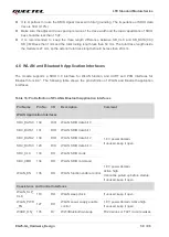
Страница 46: ... translation circuit is shown as below For the design of circuits shown in dotted lines see that shown in solid lines but pay attention to the direction of connection MCU ARM TXD RXD VDD_EXT 10K VCC_MCU 4 7K 10K VDD_EXT MAIN_TXD MAIN_RXD MAIN_RTS MAIN_CTS MAIN_DTR MAIN_RI RTS CTS GND GPIO MAIN_DCD Module GPIO EINT VDD_EXT 4 7K GND 1 nF 1 nF Figure 21 Reference Circuit with Transistor Circuit 1 Tra...

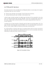
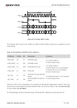
Страница 47: ...rface supports 256 512 1024 or 2048 kHz PCM_CLK at 8 kHz PCM_SYNC and also supports 4096 kHz PCM_CLK at 16 kHz PCM_SYNC In auxiliary mode the data is sampled on the falling edge of the PCM_CLK and transmitted on the rising edge The PCM_SYNC rising edge represents the MSB In this mode the PCM interface operates with a 256 512 1024 or 2048 kHz PCM_CLK and an 8 kHz 50 duty cycle PCM_SYNC The module s...

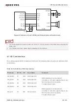
Страница 48: ... 2048 kHz PCM_CLK and 8 kHz PCM_SYNC See document 2 for more details about AT QDAI The following figure shows a reference design of PCM and I2C interfaces with external codec IC Pin Name Pin No I O Description Comment PCM_DIN 24 DI PCM data input 1 8 V power domain If unused keep it open PCM_DOUT 25 DO PCM data output PCM_SYNC 26 DIO PCM data frame sync 1 8 V power domain In master mode it is an o...

Страница 49: ...D Card Interface The module supports SDIO 3 0 interface for SD card The following table shows the pin definition of SD card interface Table 15 Pin Definition of SD Card Interface Pin Name Pin No I O Description Comment SD_DATA0 31 DIO SDIO data bit 0 SDIO signal level can be selected according to SD card supported level see SD 3 0 protocol for more details If unused keep it open SD_DATA1 30 DIO SD...

Страница 50: ...f bus resistors R7 R11 are needed to pull up the SDIO to SD_PU_VDD Value of these resistors is among 10 100 kΩ and the recommended value is 100 kΩ SD_PU_VDD should be used as the pull up power In order to adjust signal quality it is recommended to add 0 Ω resistors R1 R6 in series between the module and the SD card The bypass capacitors C1 C6 are reserved and not mounted by default All resistors a...

Страница 51: ...oth function The following table shows the pin definition of WLAN and Bluetooth application interfaces Table 16 Pin Definition of WLAN Bluetooth Application Interfaces Pin Name Pin No I O Description Comment WLAN Application Interfaces SDC_DATA0 132 DIO WLAN SDIO data bit 0 1 8 V power domain If unused keep it open SDC_DATA1 131 DIO WLAN SDIO data bit 1 SDC_DATA2 130 DIO WLAN SDIO data bit 2 SDC_D...

Страница 52: ...luetooth coexistence transmit Bluetooth Application Interfaces BT_RTS 37 DI DTE request to send signal to DCE Connect to DTE s RTS 1 8 V power domain If unused keep it open BT_TXD 38 DO Bluetooth UART transmit 1 8 V power domain If unused keep it open BT_RXD 39 DI Bluetooth UART receive BT_CTS 40 DO DTE clear to send signal from DCE Connect to DTE s CTS 1 8 V power domain Cannot be pulled up befor...

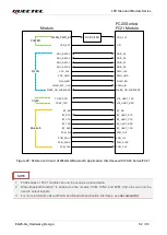
Страница 53: ...CM_CLK BT_EN BT_UART_RTS BT_UART_CTS BT_UART_RXD BT_UART_TXD PCM_OUT PCM_IN PCM_SYNC PCM_CLK VDD_EXT VIO COEX_TXD COEX_RXD LTE_UART_TXD LTE_UART_RXD COEX Bluetooth FC20 Series FC21 Module Figure 26 Reference Circuit of WLAN Bluetooth Application Interfaces with FC20 Series FC21 1 FC20 series or FC21 module can only be used as a slave device 2 When Bluetooth function is enabled on the module PCM_SY...

Страница 54: ...ation resistors within 15 24 Ω on clock traces near the module and keep the route distance from the module clock pins to termination resistors less than 5 mm Make sure the adjacent trace spacing is 2 times of the trace width and bus capacitance is less than 15 pF 4 6 2 Bluetooth Application Interface The module supports a dedicated UART interface and a PCM interface for Bluetooth application Furth...

Страница 55: ...interface are shown below IEEE802 3 compliant Supports 10 100 1000 Mbps Ethernet work mode Supports maximum 150 Mbps DL 50 Mbps UL for 4G network Supports VLAN tagging Supports IEEE1588 and Precision Time Protocol PTP Can be used to connect to external Ethernet PHY like AR8033 or to an external switch Management interfaces support dual voltage 1 8 2 85 V The following table shows the pin definitio...

Страница 56: ...d keep it open SGMII_MDIO 121 DIO SGMII management data 1 8 2 85 V power domain Require external pull up to SGMII_MDIO_VDD and the resistor should be 1 5 kΩ If unused keep it open SGMII_MDC 122 DO SGMII management data clock 1 8 2 85 V power domain If unused keep it open SGMII_MDIO_ VDD 128 PO SGMII_MDIO pull up power supply Configurable power source 1 8 2 85 V power domain If unused keep it open ...

Страница 57: ... from other sensitive circuits signals such as RF circuits analog signals etc as well as noisy signals such as clock signals DC DC signals etc Keep the maximum trace length less than 10 inches and keep skew on the differential pairs less than 20 mil The differential impedance of SGMII data trace is 100 Ω 10 and the reference ground of the area should be complete Make sure the trace spacing between...

Страница 58: ... Description Comment NET_MODE 5 DO Indicate the module s network registration mode 1 8 V power domain Cannot be pulled up before startup If unused keep it open NET_STATUS 6 DO Indicate the module s network activity status 1 8 V power domain If unused keep it open Pin Name Logic Level Changes Network Status NET_MODE Always High Registered on LTE network Always Low Others NET_STATUS Flicker slowly 2...

Страница 59: ...one according to your application demands VDD_MCU 10K Module STATUS MCU_GPIO Module STATUS VBAT 2 2K Figure 30 Reference Circuits of STATUS The status pin cannot be used as indication of module shutdown status when VBAT power supply is removed 4 9 3 MAIN_RI AT QCFG risignaltype physical can be used to configure MAIN_RI behaviors No matter on which port a URC is presented the URC will trigger the b...

Страница 60: ...ergency download mode when it is powered on In this mode the module supports firmware upgrade over USB interface Table 24 Pin Definition of USB_BOOT Interface The following figures show the reference circuit of USB_BOOT interface and timing sequence of entering emergency download mode State Response Idle MAIN_RI keeps at high level URC MAIN_RI outputs 120 ms low pulse when a new URC returns Pin Na...

Страница 61: ...500 ms VIL 0 5 V About 100 ms Figure 32 Timing Sequence for Entering Emergency Download Mode 1 Make sure that VBAT is stable before pulling down PWRKEY pin It is recommended that the time between powering up VBAT and pulling down PWRKEY pin is not less than 30 ms 2 When using MCU to control module to enter the emergency download mode please follow the above timing sequence It is not recommended to...

Страница 62: ...Bands Pin Name Pin No I O Description Comment ANT_MAIN 49 AIO Main antenna interface 50 Ω impedance ANT_DIV 35 AI Diversity antenna interface 50 Ω impedance If unused keep it open 3GPP Bands Transmit Receive Unit GSM850 824 849 869 894 MHz EGSM900 880 915 925 960 MHz DCS1800 1710 1785 1805 1880 MHz PCS1900 1850 1910 1930 1990 MHz WCDMA B1 1920 1980 2110 2170 MHz WCDMA B2 1850 1910 1930 1990 MHz WC...

Страница 63: ...2690 MHz LTE FDD B8 880 915 925 960 MHz LTE FDD B12 699 716 729 746 MHz LTE FDD B13 777 787 746 756 MHz LTE FDD B18 815 830 860 875 MHz LTE FDD B19 830 845 875 890 MHz LTE FDD B20 832 862 791 821 MHz LTE FDD B25 1850 1915 1930 1995 MHz LTE FDD B26 814 849 859 894 MHz LTE FDD B28 703 748 758 803 MHz LTE TDD B34 2010 2025 2010 2025 MHz LTE TDD B38 2570 2620 2570 2620 MHz LTE TDD B39 1880 1920 1880 1...

Страница 64: ...ed RF Receiving Sensitivity 6 SIMO is a smart antenna technology that uses a single antenna at the transmitter side and two antennas at the receiver side which can improve Rx performance Frequency Bands Max RF Output Power Min RF Output Power GSM850 EGSM900 33 dBm 2 dB 5 dBm 5 dB DCS1800 PCS1900 30 dBm 2 dB 0 dBm 5 dB GSM850 EGSM900 8 PSK 27 dBm 3 dB 5 dBm 5 dB DCS1800 PCS1900 8 PSK 26 dBm 3 dB 0 ...

Страница 65: ...FDD B3 10 MHz 97 dBm 97 dBm 98 dBm 93 3 dBm LTE FDD B4 10 MHz 96 3 dBm 96 3 dBm 99 7 dBm 96 3 dBm LTE FDD B5 10 MHz 96 3 dBm 96 4 dBm 100 dBm 94 3 dBm LTE FDD B7 10 MHz 95 5 dBm 94 8 dBm 99 2 dBm 94 3 dBm LTE FDD B8 10 MHz 97 dBm 97 dBm 101 dBm 93 3 dBm LTE FDD B12 10 MHz 97 5 dBm 98 dBm 99 8 dBm 93 3 dBm LTE FDD B13 10 MHz 97 2 dBm 97 3 dBm 98 dBm 93 3 dBm LTE FDD B18 10 MHz 96 7 dBm 96 4 dBm 101...

Страница 66: ... Antenna Interface 1 Keep a proper distance between the main antenna and the Rx diversity antenna to improve the receiving sensitivity 2 For the operation of ANT_MAIN and ANT_DIV see AT QCFG divctl in document 3 for details 3 Place the π type matching components R1 C1 and C2 R2 C3 and C4 as close to the antenna as possible LTE TDD B38 10 MHz 97 dBm 97 dBm 100 dBm 96 3 dBm LTE TDD B39 10 MHz 97 5 d...

Страница 67: ...ault The GNSS engine of the module is switched off by default It has to be switched on via AT command For more details about GNSS engine technology and configurations see document 6 Table 29 Pin Definition of GNSS Antenna Interface Table 30 GNSS Frequency A reference design of GNSS antenna is shown as below Pin Name Pin No I O Description Comment ANT_GNSS 47 AI GNSS antenna interface 50 Ω impedanc...

Страница 68: ...eded 3 It is recommended to use a passive GNSS antenna when LTE B13 is supported as the use of active antenna may generate harmonics which will affect the GNSS performance 5 2 2 GNSS Performance The following table shows the GNSS performance of the module Table 31 GNSS Performance Parameter Description Conditions Typ Unit Sensitivity Acquisition Autonomous 146 dBm Reacquisition Autonomous 156 dBm ...

Страница 69: ...M card USB interface camera module and display connector should be kept away from the antennas Use ground vias around the GNSS trace and sensitive analog signal traces to provide coplanar isolation and protection Keep 50 Ω characteristic impedance for the ANT_GNSS trace 5 3 RF Routing Guidelines For user s PCB the characteristic impedance of all RF traces should be controlled to 50 Ω The impedance...

Страница 70: ...le Series EG25 GL_Hardware_Design 69 96 Figure 35 Microstrip Design on a 2 layer PCB Figure 36 Coplanar Waveguide Design on a 2 layer PCB Figure 37 Coplanar Waveguide Design on a 4 layer PCB Layer 3 as Reference Ground ...

Страница 71: ...nded trace angle is 135 There should be clearance under the signal pin of the antenna connector or solder joint The reference ground of RF traces should be complete Meanwhile adding some ground vias around RF traces and the reference ground could help to improve RF performance The distance between the ground vias and RF traces should be not less than twice the width of RF signal traces 2 W Keep RF...

Страница 72: ...n it is recommended to use the U FL R SMT connector provided by Hirose Figure 39 Dimensions of the Receptacle Unit mm U FL LP series mated plugs listed in the following figure can be used to match the U FL R SMT connector Passive antenna gain 0 dBi Active antenna noise figure 1 5 dB Active antenna gain 0 dBi Active antenna embedded LNA gain 17 dB GSM WCDMA LTE VSWR 2 Efficiency 30 Max input power ...

Страница 73: ...G25 GL_Hardware_Design 72 96 Figure 40 Specifications of Mated Plugs The following figure describes the space factor of mated connectors Figure 41 Space Factor of Mated Connectors Unit mm For more details visit http www hirose com ...

Страница 74: ... for power supply and voltage on digital and analog pins of the module are listed in the following table Table 33 Absolute Maximum Ratings Parameter Min Max Unit VBAT_RF VBAT_BB 0 3 4 7 V USB_VBUS 0 3 5 5 V Peak Current of VBAT_BB 0 8 A Peak Current of VBAT_RF 1 8 A Voltage at Digital Pins 0 3 2 3 V Voltage at ADC0 0 VBAT_BB V Voltage at ADC1 0 VBAT_BB V ...

Страница 75: ... burst transmission Maximum power control level on EGSM900 400 mV IVBAT Peak supply current during transmission slot Maximum power control level on EGSM900 1 8 2 0 A USB_VBUS USB connection detection 3 0 5 0 5 25 V Description Conditions Typ Unit Power off Power down 7 μA Sleep State AT CFUN 0 USB disconnected 1 3 mA AT CFUN 0 USB suspended 1 5 mA AT CFUN 4 USB disconnected 1 3 mA AT CFUN 4 USB su...

Страница 76: ...32 USB disconnected 3 7 mA LTE FDD PF 64 USB disconnected 2 6 mA LTE FDD PF 64 USB suspended 2 8 mA LTE FDD PF 128 USB disconnected 2 0 mA LTE FDD PF 256 USB disconnected 1 7 mA LTE TDD PF 32 USB disconnected 4 0 mA LTE TDD PF 64 USB disconnected 2 6 mA LTE TDD PF 64 USB suspended 2 9 mA LTE TDD PF 128 USB disconnected 2 0 mA LTE TDD PF 256 USB disconnected 1 6 mA Idle State EGSM900 DRX 5 USB disc...

Страница 77: ...9 08 dBm 470 mA GSM850 1DL 4UL 27 93 dBm 580 mA DCS1800 4DL 1UL 28 69 dBm 180 mA DCS1800 3DL 2UL 28 25 dBm 280 mA DCS1800 2DL 3UL 26 28 dBm 350 mA DCS1800 1DL 4UL 25 51 dBm 460 mA PCS1900 4DL 1UL 29 21 dBm 170 mA PCS1900 3DL 2UL 28 30 dBm 270 mA PCS1900 2DL 3UL 26 86 dBm 350 mA PCS1900 1DL 4UL 25 57 dBm 440 mA EDGE Data Transfer GNSS OFF EGSM900 4DL 1UL 26 11 dBm 190 mA EGSM900 3DL 2UL 24 93 dBm 3...

Страница 78: ... WCDMA Data Transfer GNSS OFF WCDMA B1 HSDPA 22 6 dBm 600 mA WCDMA B1 HSUPA 22 4 dBm 580 mA WCDMA B2 HSDPA 22 73 dBm 700 mA WCDMA B2 HSUPA 22 89 dBm 690 mA WCDMA B4 HSDPA 22 72 dBm 630 mA WCDMA B4 HSUPA 22 24 dBm 610 mA WCDMA B5 HSDPA 22 48 dBm 750 mA WCDMA B5 HSUPA 22 dBm 740 mA WCDMA B6 HSDPA 22 38 dBm 760 mA WCDMA B6 HSUPA 21 95 dBm 720 mA WCDMA B8 HSDPA 22 45 dBm 745 mA WCDMA B8 HSUPA 22 dBm 7...

Страница 79: ...2 dBm 910 mA LTE FDD B20 23 16 dBm 910 mA LTE FDD B25 23 26 dBm 820 mA LTE FDD B26 23 06 dBm 920 mA LTE FDD B28 23 55 dBm 860 mA LTE TDD B34 22 75 dBm 380 mA LTE TDD B38 22 86 dBm 450 mA LTE TDD B39 22 82 dBm 360 mA LTE TDD B40 22 94 dBm 400 mA LTE TDD B41 22 90 dBm 490 mA LTE FDD B66 23 40 dBm 780 mA GSM Voice Call EGSM900 PCL 5 32 22 dBm 270 mA EGSM900 PCL 12 19 71 dBm 140 mA EGSM900 PCL 19 3 09...

Страница 80: ...e product design Table 36 Electrostatic Discharge Characteristics 25 º C 45 Relative Humidity DCS1800 PCL 0 28 91 dBm 180 mA DCS1800 PCL 7 15 83 dBm 140 mA DCS1800 PCL 15 2 91 dBm 80 mA PCS1900 PCL 0 29 31 dBm 170 mA PCS1900 PCL 7 15 81 dBm 140 mA PCS1900 PCL 15 2 75 dBm 78 mA WCDMA Voice Call WCDMA B1 23 65 dBm 670 mA WCDMA B2 23 96 dBm 750 mA WCDMA B4 23 77 dBm 700 mA WCDMA B5 23 51 dBm 830 mA W...

Страница 81: ...e remains the ability to establish and maintain functions such as voice SMS data transmission etc without any unrecoverable malfunction Radio spectrum and radio network are not influenced while one or more specifications such as Pout may exceed the specified tolerances of 3GPP When the temperature returns to the operating temperature range the module meets 3GPP specifications again Parameter Min T...

Страница 82: ... 7 Mechanical Information This chapter describes the mechanical dimensions of the module All dimensions are measured in mm and the dimensional tolerances are 0 2 mm unless otherwise specified 7 1 Mechanical Dimensions Figure 42 Module Top and Side Dimensions ...

Страница 83: ...LTE Standard Module Series EG25 GL_Hardware_Design 82 96 Figure 43 Bottom Dimensions Bottom View The package warpage level of the module conforms to the JEITA ED 7306 standard NOTE ...

Страница 84: ... 96 7 2 Recommended Footprint Figure 44 Recommended Footprint Top View 1 The keepout area should not be designed 2 Keep at least 3 mm between the module and other components on the motherboard to improve soldering quality and maintenance convenience NOTE ...

Страница 85: ...module please keep about 3 mm between the module and other components in the host PCB 3 LGA form factor is used for EG25 GL module while LCC is recommended only in the compatible design with EC25 series EC21 series EC20 CE EG21 G EG25 G EC200A series modules If you use LCC form factor you should choose the stencil matched with LGA package instead of that matched with LCC package For more details s...

Страница 86: ...n 85 96 7 4 Top and Bottom Views Figure 46 Top and Bottom Views of the Module Images above are for illustration purpose only and may differ from the actual module For authentic appearance and label please refer to the module received from Quectel NOTE ...

Страница 87: ...a dry cabinet 4 The module should be pre baked to avoid blistering cracks and inner layer separation in PCB under the following circumstances The module is not stored in Recommended Storage Condition Violation of the third requirement mentioned above Vacuum sealed packaging is broken or the packaging has been removed for over 24 hours Before module repairing 5 If needed the pre baking should follo...

Страница 88: ... PCB Apply proper force on the squeegee to produce a clean stencil surface on a single pass To guarantee module soldering quality the thickness of stencil for the module is recommended to be 0 13 0 15 mm For more details see document 8 The peak reflow temperature should be 235 246 º C with 246 º C as the absolute maximum reflow temperature To avoid damage to the module caused by repeated heating i...

Страница 89: ...e for any situation that you are not sure about or any process e g selective soldering ultrasonic soldering that is not mentioned in document 8 8 3 Packaging Specifications This chapter describes only the key parameters and process of packaging All figures below are for reference only The appearance and structure of the packaging materials are subject to the actual delivery The module adopts carri...

Страница 90: ...8 3 1 Carrier Tape Dimension details are as follow Figure 48 Carrier Tape Dimension Drawing Table 39 Carrier Tape Dimension Table Unit mm 8 3 2 Plastic Reel Figure 49 Plastic Reel Dimension Drawing W P T A0 B0 K0 K1 F E 44 44 0 35 32 5 29 5 3 0 3 8 20 2 1 75 ...

Страница 91: ...ape and use the cover tape to cover it then wind the heat sealed carrier tape to the plastic reel and use the protective tape for protection 1 plastic reel can load 250 modules Place the packaged plastic reel 1 humidity indicator card and 1 desiccant bag into a vacuum bag vacuumize it Place the vacuum packed plastic reel into the pizza box øD1 øD2 W 330 100 44 5 ...

Страница 92: ...LTE Standard Module Series EG25 GL_Hardware_Design 91 96 Put 4 packaged pizza boxes into 1 carton box and seal it 1 carton box can pack 1000 modules Figure 50 Packaging Process ...

Страница 93: ... Quectel_EC2x EG9x EG2x G L _Series_Power_Management_Application_Note 5 Quectel_EG25 GL_Reference_Design 6 Quectel_EC2x EG2x G L EG9x EM05_Series_GNSS_Application_Note 7 Quectel_RF_Layout_Application_Note 8 Quectel_Module_Secondary_SMT_Application_Note Abbreviation Description AMR Adaptive Multi rate AMR WB Adaptive Multi Rate Wideband bps Bits Per Second CHAP Challenge Handshake Authentication Pr...

Страница 94: ...VB Evaluation Board FDD Frequency Division Duplex FR Full Rate FTP File Transfer Protocol FTPS FTP over SSL GLONASS Global Navigation Satellite System Russia GMSK Gaussian Minimum Shift Keying GNSS Global Navigation Satellite System GPS Global Positioning System GSM Global System for Mobile Communications HR Half Rate HSPA High Speed Packet Access HSDPA High Speed Downlink Packet Access HSUPA High...

Страница 95: ...edia Messaging Service MO Mobile Originated MQTT Message Queuing Telemetry Transport MS Mobile Station GSM engine MSL Moisture Sensitivity Level MT Mobile Terminated NITZ Network Identity and Time Zone NMEA NMEA National Marine Electronics Association 0183 Interface Standard NTP Network Time Protocol PAP Password Authentication Protocol PCB Printed Circuit Board PCM Pulse Code Modulation PDA Perso...

Страница 96: ...I Serial Gigabit Media Independent Interface SIMO Single Input Multiple Output SMD Surface Mount Device SMS Short Message Service SMTP Simple Mail Transfer Protocol SMTPS Simple Mail Transfer Protocol Secure SSL Secure Sockets Layer TCP Transmission Control Protocol TDD Time Division Duplexing TVS Transient Voltage Suppressor TX Transmitting Direction UDP User Datagram Protocol UL Uplink UMTS Univ...

Страница 97: ... VIHmin Minimum High level Input Voltage VILmax Maximum Low level Input Voltage VILmin Minimum Low level Input Voltage VOHmax Maximum High level Output Voltage VOHmin Minimum High level Output Voltage VOLmax Maximum Low level Output Voltage VOLmin Minimum Low level Output Voltage VSWR Voltage Standing Wave Ratio WCDMA Wideband Code Division Multiple Access WLAN Wireless Local Area Network ...

Страница 98: ...nal emissions other than what is permitted in Part 15 Subpart B or emissions are complaint with the transmitter s rule s The Grantee will provide guidance to the host manufacturer for Part 15 B requirements if needed Important Note notice that any deviation s from the defined parameters of the antenna trace as described by the instructions require that the host product manufacturer must notify to ...

Страница 99: ...he end product including the transmitter and obtaining a separate FCC IC authorization To comply with FCC regulations limiting both maximum RF output power and human exposure to RF radiation maximum antenna gain including cable loss must not exceed Technology Frequency Range MHz Antenna Type Max Peak Gain dBi GSM 850 824 849 Dipole 6 3 PCS 1900 1850 1910 11 9 WCDMA Band II 1850 1910 9 9 WCDMA Band...

Страница 100: ...ware not to provide information to the end user regarding how to install or remove this RF module in the user s manual of the end product which integrates this module The end user manual shall include all required regulatory information warning as show in this manual ...

Страница 101: ...asures Reorient or relocate the receiving antenna Increase the separation between the equipment and receiver Connect the equipment into an outlet on a circuit different from that to which the receiver is connected Consult the dealer or an experienced radio TV technician for help Any changes or modifications not expressly approved by the party responsible for compliance could void the user s author...

Страница 102: ...nna As long as 2 conditions above are met further transmitter test will not be required However the OEM integrator is still responsible for testing their end product for any additional compliance requirements required with this module installed Radiation Exposure Statement This equipment complies with FCC radiation exposure limits set forth for an uncontrolled environment This equipment should be ...

Страница 103: ...its set forth for an uncontrolled environment This equipment should be installed and operated with minimum distance 20 cm between the radiator your body Déclaration d exposition aux radiations Cet équipement est conforme aux limites d exposition aux rayonnements ISED établies pour un environnement non contrôlé Cet équipement doit être installé et utilisé avec un minimum de 20 cm de distance entre ...

Страница 104: ... the transmitter and obtaining a separate Canada authorization NOTE IMPORTANTE Dans le cas où ces conditions ne peuvent être satisfaites par exemple pour certaines configurations d ordinateur portable ou de certaines co localisation avec un autre émetteur l autorisation du Canada n est plus considéré comme valide et l ID IC ne peut pas être utilisé sur le produit final Dans ces circonstances l int...

Страница 105: ... required regulatory information warning as show in this manual Manuel d information à l utilisateur final L intégrateur OEM doit être conscient de ne pas fournir des informations à l utilisateur final quant à la façon d installer ou de supprimer ce module RF dans le manuel de l utilisateur du produit final qui intègre ce module Le manuel de l utilisateur final doit inclure toutes les informations...

Отзывы: