background image

LTE-A  Module  Series 

                                                                                                                                EG12  Hardware  Design


EG12_Hardware_Design                                                                                                                          94 / 97


9


Appendix A References 


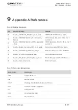
Table 49: Related Documents 


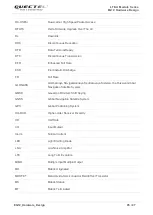
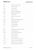
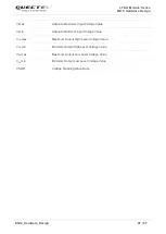
Table 50: Terms and Abbreviations 

SN 

Document Name 

Remark 

[1] 

Quectel_UMTS&LTE_EVB_R2.0_User_Guide 

UMTS&LTE EVB R2.0 User Guide 

[2] 

Quectel_EM12&EG12&EG18_AT_Commands_ 

Manual 

AT Commands Manual for EM12, EG12 

and EG18 

[3] 

Quectel_EM12&EG12&EG18_GNSS_Application

_Note 

GNSS  Application  Note  for  EM12,  EG12 

and EG18 

[4] 

Quectel_Module_Secondary_SMT_User_Guide 

Module Secondary SMT User Guide 

[5] 

Quectel_EG12&EG18_Reference_Design 

Reference Design for EG12 and EG18 

[6] 

Quectel_RF_Layout_Application_Note 

RF Layout Application Note 

[7] 

Quectel_LTE_Module_Thermal_Design_Guide 

Thermal Design Guide for LTE Modules 

[8] 

Quectel_EG12_CA_Feature 

EG12 CA Feature 

Abbreviation 

Description 

AMR 

Adaptive Multi-rate 

bps 

Bits Per Second 

CHAP   

Challenge Handshake Authentication Protocol 

CPE 

Customer Premises Equipment 


CS   

Coding Scheme 

CSD   

Circuit Switched Data 

CTS   

Clear To Send 

Содержание EG12 Series

Страница 1: ...EG12 Hardware Design LTE A Module Series Rev EG12_Hardware_Design_V1 1 Date 2019 09 30 Status Released www quectel com ...

Страница 2: ...E INFORMATION PROVIDED IS BASED UPON CUSTOMERS REQUIREMENTS QUECTEL MAKES EVERY EFFORT TO ENSURE THE QUALITY OF THE INFORMATION IT MAKES AVAILABLE QUECTEL DOES NOT MAKE ANY WARRANTY AS TO THE INFORMATION CONTAINED HEREIN AND DOES NOT ACCEPT ANY LIABILITY FOR ANY INJURY LOSS OR DAMAGE OF ANY KIND INCURRED BY USE OF OR RELIANCE UPON THE INFORMATION ALL INFORMATION SUPPLIED HEREIN IS SUBJECT TO CHANG...

Страница 3: ...al 1 1 2019 09 30 Archibald JIANG Xavier XIA 1 Updated the operation temperature range of EG12 in Table 2 and Table 41 2 Restricted the function of pins 159 162 and 172 GPIO_3 GPIO_4 and GPIO_5 to external tuner control only Table 4 Chapter 3 20 3 Removed the power consumption data of EG12 CA combinations as more specific data are provided in Quectel_EG12_CA_Feature Chapter 6 4 ...

Страница 4: ... with USB Remote Wakeup Function 33 3 5 1 3 USB Application with USB Suspend Resume and RI Function 34 3 5 1 4 USB Application without USB Suspend Function 34 3 5 2 Airplane Mode 35 3 6 Power Supply 36 3 6 1 Power Supply Pins 36 3 6 2 Decrease Voltage Drop 37 3 6 3 Reference Design for Power Supply 38 3 6 4 Monitor the Power Supply 38 3 7 Turn on and off Scenarios 38 3 7 1 Turn on the Module Using...

Страница 5: ...Pin Definition 67 5 1 2 Operating Frequency 67 5 1 3 Reference Design of RF Antenna Interfaces 69 5 2 GNSS Antenna Interface 70 5 2 1 Pin Definition 70 5 2 2 GNSS Frequency 71 5 2 3 Reference Design of GNSS Antenna Interface 71 5 3 Reference Design of RF Layout 72 5 4 Antenna Installation 74 5 4 1 Antenna Requirements 74 5 4 2 Recommended RF Connector for Antenna Installation 75 6 Electrical Relia...

Страница 6: ...eration 83 7 Mechanical Dimensions 86 7 1 Mechanical Dimensions of the Module 86 7 2 Recommended Footprint 88 7 3 Top and Bottom Views of the Module 89 8 Storage Manufacturing and Packaging 90 8 1 Storage 90 8 2 Manufacturing and Soldering 91 8 3 Packaging 92 9 Appendix A References 94 ...

Страница 7: ...DC INTERFACES 55 TABLE 20 CHARACTERISTICS OF ADC INTERFACES 55 TABLE 21 PIN DEFINITION OF NETWORK CONNECTION STATUS ACTIVITY INDICATOR 56 TABLE 22 WORKING STATE OF THE NETWORK CONNECTION STATUS ACTIVITY INDICATOR 56 TABLE 23 PIN DEFINITION OF STATUS 57 TABLE 24 BEHAVIOR OF THE RI 58 TABLE 25 PIN DEFINITION OF THE PCIE INTERFACE 58 TABLE 26 PIN DEFINITION OF SDIO INTERFACE 61 TABLE 27 PIN DEFINITIO...

Страница 8: ...RRENT CONSUMPTION 79 TABLE 44 RF OUTPUT POWER 81 TABLE 45 EG12 GT CONDUCTED RF RECEIVING SENSITIVITY 82 TABLE 46 EG12 EA CONDUCTED RF RECEIVING SENSITIVITY 82 TABLE 47 ELECTROSTATIC DISCHARGE CHARACTERISTICS 83 TABLE 48 RECOMMENDED THERMAL PROFILE PARAMETERS 91 TABLE 49 RELATED DOCUMENTS 94 TABLE 50 TERMS AND ABBREVIATIONS 94 ...

Страница 9: ... SIM INTERFACE WITH AN 8 PIN U SIM CARD CONNECTOR 44 FIGURE 19 REFERENCE CIRCUIT OF A U SIM INTERFACE WITH A 6 PIN U SIM CARD CONNECTOR 44 FIGURE 20 REFERENCE CIRCUIT OF USB APPLICATION 46 FIGURE 21 LEVEL TRANSLATION REFERENCE CIRCUIT WITH AN IC 50 FIGURE 22 LEVEL TRANSLATION REFERENCE CIRCUIT WITH MOSFETS 50 FIGURE 23 TIMING OF SPI INTERFACE 51 FIGURE 24 PRIMARY MODE TIMING 53 FIGURE 25 AUXILIARY...

Страница 10: ...TSINK DESIGN HEATSINK AT THE TOP OF THE MODULE 84 FIGURE 43 REFERENCED HEATSINK DESIGN HEATSINK AT THE BACKSIDE OF CUSTOMERS PCB 84 FIGURE 44 MODULE TOP AND SIDE DIMENSIONS 86 FIGURE 45 MODULE BOTTOM DIMENSIONS TOP VIEW 87 FIGURE 46 RECOMMENDED FOOTPRINT TOP VIEW 88 FIGURE 47 TOP VIEW OF THE MODULE 89 FIGURE 48 BOTTOM VIEW OF THE MODULE 89 FIGURE 49 REFLOW SOLDERING THERMAL PROFILE 91 FIGURE 50 TA...

Страница 11: ...tomers applications This document helps customers quickly understand module interface specifications electrical and mechanical details as well as other related information of EG12 To facilitate application designs it also includes some reference designs for customers reference The document coupled with application notes and user guides makes it easy to design and set up mobile applications with EG...

Страница 12: ...onsult the airline staff for more restrictions on the use of wireless devices on boarding the aircraft Wireless devices may cause interference on sensitive medical equipment so please be aware of the restrictions on the use of wireless devices when in hospitals clinics or other healthcare facilities Cellular terminals or mobiles operating over radio signals and cellular network cannot be guarantee...

Страница 13: ...ed on the region or operator The following table shows the frequency bands CA combinations 3 and GNSS types of EG12 module Table 1 Frequency Bands CA Combinations and GNSS Types of EG12 Module Mode EG12 GT EG12 EA EG12 NA LTE FDD with Rx diversity Not supported B1 B3 B5 B7 B8 B20 B28 B2 B4 B5 B7 B12 B13 B14 B17 B25 B26 B29 4 B30 B66 B71 LTE TDD with Rx diversity B42 B43 B48 B38 B40 B41 B41 2 CA DL...

Страница 14: ...ve security 4G router CPE wireless POS Terminal mobile computing device PDA phone and tablet PC EG12 is an SMD type module and can be embedded in applications through its 299 LGA pins B38 B38 B40 B40 B41 B41 3 CA DL B42 B42 B42 B48 B48 B48 B1 B3 B3 B5 B7 B8 B20 B28 B38 B41 B1 B40 B40 B1 B41 B41 B1 B7 B20 B3 B3 B7 B20 B28 B3 B7 B7 B8 B20 B28 B3 B40 B40 B3 B41 B41 B7 B7 B20 B28 B40 B40 B40 B41 B41 B...

Страница 15: ...D Max 600Mbps DL 150Mbps UL TDD Max 430Mbps DL 90Mbps UL UMTS Features Support 3GPP R9 DC HSDPA DC HSUPA HSPA HSDPA HSUPA and WCDMA Support QPSK 16 QAM and 64 QAM modulation DC HSDPA Max 42Mbps DC HSUPA Max 11 2Mbps WCDMA Max 384Kbps DL 384Kbps UL Internet Protocol Features Support PPP QMI TCP UDP FTP HTTP NTP PING HTTPS SMTP MMS FTPS SMTPS SSL protocols Support the PAP Password Authentication Pro...

Страница 16: ...control Debug UART interface Used for Linux console and log output 115200bps baud rate BT UART interface Used for Bluetooth communication and can be multiplexed into SPI interface 115200bps baud rate PCIe 1 Interface Comply with PCI Express Specification Revision 2 1 and support 5Gbps per lane Used for data transmission Rx diversity Support LTE WCDMA Rx diversity and LTE HO diversity GNSS Features...

Страница 17: ...o be realized Only one or more parameters like Pout might reduce in their value and exceed the specified tolerances When the temperature returns to normal operating temperature levels the module will meet 3GPP specifications again 2 3 Functional Diagram The following figure shows a block diagram of EG12 and illustrates the major functional parts Power management Baseband LPDDR2 SDRAM NAND Flash Ra...

Страница 18: ...ET_N 38 4M XO STATUS GPIOs Control QLINK Control Tx PRx DRx Baseband PCIe I2S_MCLK SDIO BT_UART SPI ANT_GNSS ANT_MIMO1 VDD_RF Figure 1 Functional Diagram 2 4 Evaluation Board In order to facilitate application development with EG12 conveniently Quectel supplies an evaluation board EVB USB to RS 232 converter cable earphone antenna and other peripherals to control or test the module For more detail...

Страница 19: ...interfaces and indication signals of EG12 Power supply U SIM interfaces USB interface UART interfaces SPI interface 1 PCM and I2C interfaces ADC interfaces Network status indication Module operation status indication PCIe interface SDIO interface Antenna tuner control interfaces USB_BOOT interface GPIOs 1 means under development 2 1 SPI interface is multiplexed from BT UART interface 3 2 Pin Assig...

Страница 20: ...O Pins ADC Pins UART Pins SPI Pins ANT Pins CLK Pins RESET_N PWRKEY BT_EN WLAN_PWR_EN USIM1_DET USIM1_CLK USIM1_DATA USIM1_VDD USIM1_RST USB_VBUS USB_DM USB_DP USB_ID USB_SS_TX_M USB_SS_TX_P USB_SS_RX_P USB_SS_RX_M I2C_SDA I2C_SCL SD_VDD SD_DATA2 SD_DATA3 SD_DATA0 SD_DATA1 SD_CMD SD_DET SD_CLK CTS RTS RXD DCD TXD RI DTR PCM_SYNC PCM_CLK PCM_IN PCM_OUT USIM2_DATA USIM2_RST USIM2_DET USIM2_CLK VBAT_...

Страница 21: ...escription AI Analog Input AO Analog Output DI Digital Input DO Digital Output IO Bidirectional OD Open Drain PI Power Input PO Power Output Power Supply Pin Name Pin No I O Description DC Characteristics Comment VBAT_BB 155 156 PI Power supply for the module s baseband part Vmax 4 3V Vmin 3 3V Vnorm 3 8V It must be provided with sufficient current up to 1 0A VBAT_RF 85 86 87 88 PI Power supply fo...

Страница 22: ... 85V IOmax 120mA GND 10 13 16 17 24 30 31 35 39 44 45 54 55 63 64 69 70 75 76 81 84 89 90 92 94 96 100 102 106 108 112 114 118 120 126 128 133 141 142 148 153 154 157 158 167 174 177 178 181 184 187 191 196 202 208 214 299 Ground Turn on off Pin Name Pin No I O Description DC Characteristics Comment RESET_N 1 DI Reset the module VIHmax 2 1V VIHmin 1 3V VILmax 0 5V 1 8V power domain Pulled up inter...

Страница 23: ...me Pin No I O Description DC Characteristics Comment USIM1_DET 25 DI U SIM1 card insertion detection VILmin 0 3V VILmax 0 6V VIHmin 1 2V VIHmax 2 0V 1 8V power domain If unused keep it open USIM1_VDD 26 PO Power supply for U SIM1 card IOmax 50mA For 1 8V U SIM Vmax 1 9V Vmin 1 7V For 3 0V U SIM Vmax 3 05V Vmin 2 75V Either 1 8V or 3 0V is supported by the module automatically USIM1_CLK 27 DO Clock...

Страница 24: ...V VIHmin 2V VOLmax 0 4V VOHmin 2 3V If U SIM2 interface is unused keep it open USIM2_DET 78 DI U SIM2 card insertion detection VILmin 0 3V VILmax 0 6V VIHmin 1 2V VIHmax 2 0V 1 8V power domain If U SIM2 interface is unused keep it open USIM2_RST 79 DO Reset signal of U SIM2 card For 1 8V U SIM VOLmax 0 4V VOHmin 1 45V For 3 0V U SIM VOLmax 0 4V VOHmin 2 3V If U SIM2 interface is unused keep it ope...

Страница 25: ...min 0 3V VILmax 0 6V VIHmin 1 2V VIHmax 2 0V 1 8V power domain If unused keep it open OTG_PWR_ EN 143 DO OTG power control VOLmax 0 45V VOHmin 1 35V SDIO Interface Pin Name Pin No I O Description DC Characteristics Comment SD_VDD 46 PO SD card application SDIO pull up power source eMMC application Keep it open when used for eMMC For 1 8V SD card Vmax 1 9V Vmin 1 75V For 3 0V SD card Vmax 3 05V Vmi...

Страница 26: ...stics Comment CTS 56 DO Clear to send VOLmax 0 45V VOHmin 1 35V 1 8V power domain If unused keep it open RTS 57 DI Request to send VILmin 0 3V VILmax 0 6V VIHmin 1 2V VIHmax 2 0V 1 8V power domain If unused keep it open RXD 58 DI Receive data VILmin 0 3V VILmax 0 6V VIHmin 1 2V VIHmax 2 0V 1 8V power domain If unused keep it open DCD 59 DO Data carrier detection VOLmax 0 45V VOHmin 1 35V 1 8V powe...

Страница 27: ...Pin Name Pin No I O Description DC Characteristics Comment BT_EN 3 DO BT function enable control VOLmax 0 45V VOHmin 1 35V 1 8V power domain If unused keep it open BT_TXD 163 DO Transmit data VOLmax 0 45V VOHmin 1 35V 1 8V power domain If unused keep it open BT UART interface pin by default Can be multiplexed into SPI_MOSI BT_CTS 164 DO Clear to send VOLmax 0 45V VOHmin 1 35V 1 8V power domain If ...

Страница 28: ...on VOLmax 0 45V VOHmin 1 35V VILmin 0 3V VILmax 0 6V VIHmin 1 2V VIHmax 2 0V 1 8V power domain In master mode it is an output signal In slave mode it is an input signal If unused keep it open PCM_IN 66 DI PCM data input VILmin 0 3V VILmax 0 6V VIHmin 1 2V VIHmax 2 0V 1 8V power domain If unused keep it open PCM_CLK 67 IO PCM clock VOLmax 0 45V VOHmin 1 35V VILmin 0 3V VILmax 0 6V VIHmin 1 2V VIHma...

Страница 29: ...e Pin No I O Description DC Characteristics Comment WLAN_PWR_EN 5 DO WLAN power supply enable control VOLmax 0 45V VOHmin 1 35V 1 8V power domain If unused keep it open COEX_UART_TX 145 DO LTE WLAN coexistence signal VOLmax 0 45V VOHmin 1 35V 1 8V power domain If unused keep it open COEX_UART_RX 146 DI LTE WLAN coexistence signal VILmin 0 3V VILmax 0 6V VIHmin 1 2V VIHmax 2 0V 1 8V power domain If...

Страница 30: ...ndard specifications Require differential impedance of 95Ω PCIE_REF CLK_M 180 AI AO Input Output PCIe reference clock PCIE_TX_M 182 AO PCIe transmission PCIE_TX_P 183 AO PCIe transmission PCIE_RX_M 185 AI PCIe receiving PCIE_RX_P 186 AI PCIe receiving PCIE_CLK_ REQ_N 188 IO PCIe clock request VOLmax 0 45V VOHmin 1 35V VILmin 0 3V VILmax 0 6V VIHmin 1 2V VIHmax 2 0V In master mode it is an input si...

Страница 31: ...max 0 45V VOHmin 1 35V If unused keep them open RFFE_DATA 73 IO VOLmax 0 45V VOHmin 1 35V VILmin 0 3V VILmax 0 6V VIHmin 1 2V VIHmax 2 0V GPIO_3 159 IO GPIO interfaces dedicated for external tuner control VOLmax 0 45V VOHmin 1 35V VILmin 0 3V VILmax 0 6V VIHmin 1 2V VIHmax 2 0V If unused keep them open GPIO_4 161 IO GPIO_5 172 IO Other Pins Pin Name Pin No I O Description DC Characteristics Commen...

Страница 32: ...sed keep it open RESERVED Pins Pin Name Pin No I O Description DC Characteristics Comment RESERVED 4 6 9 11 12 14 15 18 23 72 91 95 134 176 192 195 197 201 209 213 Reserved Keep these pins unconnected Mode Details Normal Operation mode Idle Software is active The module has registered on the network and it is ready to send and receive data Talk Data Network connection is ongoing In this mode the p...

Страница 33: ...ure of EG12 3 5 1 1 UART Application If the host communicates with the module via UART interfaces the following preconditions can let the module enter sleep mode Keep DTR at high level pulled up by default Execute AT QSCLK 1 command to enable sleep mode Airplane Mode AT CFUN 4 command or driving W_DISABLE low can set the module to airplane mode In this case RF function will be invalid Sleep Mode I...

Страница 34: ...ut RI behavior 3 5 1 2 USB Application with USB Remote Wakeup Function If the host supports USB suspend resume and remote wakeup function the following three preconditions must be met to let the module enter the sleep mode Keep DTR at high level pulled up by default Execute AT QSCLK 1 command to enable the sleep mode The host s USB bus which is connected with the module s USB interface has entered...

Страница 35: ...K 1 command to enable the sleep mode The host s USB bus which is connected with the module s USB interface has entered suspend state The following figure shows the connection between the module and the host USB_VBUS USB Interface VDD USB Interface Module Host GND GND RI EINT Figure 6 Sleep Mode Application with RI Sending data to EG12 through USB will wake up the module When EG12 has a URC to repo...

Страница 36: ... 2 Airplane Mode EG12 provides a W_DISABLE signal to disable or enable airplane mode through hardware operation The W_DISABLE pin is pulled up by default Driving it low will let the module enter airplane mode In airplane mode the RF function will be disabled The RF function can also be enabled or disabled through software AT commands The following table shows the RF function status of the module T...

Страница 37: ... are two separate voltage domains for VBAT Four VBAT_RF pins for module s RF part Two VBAT_BB pins for module s baseband part The following table shows details of VBAT pins and ground pins Table 7 VBAT and GND Pins Pin Name Pin No Description Min Typ Max Unit VBAT_RF 85 86 87 88 Power supply for the module s RF part 3 3 3 8 4 3 V VBAT_BB 155 156 Power supply for the module s baseband part 3 3 3 8 ...

Страница 38: ...se three ceramic capacitors 100nF 33pF 10pF for composing the MLCC array and place these capacitors close to VBAT pins The main power supply from an external application has to be a single voltage source and can be expanded to two sub paths with star structure The width of VBAT_BB trace should be no less than 1mm and the width of VBAT_RF trace should be no less than 2mm In principle the longer the...

Страница 39: ...he following figure shows a reference design for 5V input power source In this design output of the power supply is about 3 8V and the maximum load current is 3A DC_IN MIC29302WU IN OUT EN GND ADJ 2 4 1 3 5 VBAT 100nF 470uF 100nF 100K 47K 470uF 470R 51K 1 1 4 7K 47K VBAT_EN Figure 10 Reference Circuit of Power Supply In order to avoid damaging internal flash please do not switch off the power supp...

Страница 40: ...n on pulse PWRKEY 4 7K 47K 500ms Figure 11 Turn on the Module with a Driving Circuit Another way to control the PWRKEY is using a button directly When pressing the key electrostatic strike may generate from fingers Therefore it is necessary to place a TVS component nearby the button for ESD protection A reference circuit is shown in the following figure PWRKEY S1 Close to S1 TVS Figure 12 Turn on ...

Страница 41: ...iming of Turning on Module Please ensure that VBAT is stable for no less than 30ms before pulling down the PWRKEY 3 7 2 Turn off the Module The following two methods can be used to turn off the module using PWRKEY or AT QPOWD command 3 7 2 1 Turn off the Module Using PWRKEY Driving PWRKEY low for at least 800ms the module will execute power down procedure after the PWRKEY is released The turn off ...

Страница 42: ...ease do not switch off the power supply when the module works normally Only after the module is shut down by PWRKEY or AT command the power supply can be cut off 2 When turning off module with AT command please keep PWRKEY at high level after the execution of power off command Otherwise the module will be turned on again after successful turn off 3 8 Reset the Module The module can be reset by dri...

Страница 43: ... as below Reset pulse RESET_N 4 7K 47K 250ms 600ms Figure 15 Reference Circuit of RESET_N with a Driving Circuit RESET_N S2 Close to S2 TVS Figure 16 Reference Circuit of RESET_N with a Button The reset scenario is illustrated in the following figure VIL 0 5V VIH 1 3V VBAT 250ms Resetting Module Status Running RESET_N Restart 600ms Figure 17 Timing of Resetting the Module ...

Страница 44: ...in No I O Description Comment USIM1_DET 25 DI U SIM1 card insertion detection USIM1_VDD 26 PO Power supply for U SIM1 card Either 1 8V or 3 0V is supported by the module automatically USIM1_CLK 27 DO Clock signal of U SIM1 card USIM1_RST 28 DO Reset signal of U SIM1 card USIM1_DATA 29 IO Data signal of U SIM1 card USIM2_VDD 74 PO Power supply for U SIM2 card Either 1 8V or 3 0V is supported by the...

Страница 45: ...ATA USIM_DET 22R 22R 22R VDD_EXT 51K 100nF U SIM Card Connector GND GND VCC RST CLK IO VPP GND USIM_VDD 15K NM NM NM CD1 CD2 Figure 18 Reference Circuit of a U SIM Interface with an 8 Pin U SIM Card Connector If U SIM card detection function is not needed please keep USIM_DET pins unconnected A reference circuit for a U SIM interface with a 6 pin U SIM card connector is illustrated in the followin...

Страница 46: ... peripheral circuit should be close to the U SIM card connector The pull up resistor on USIM_DATA line can improve anti jamming capability when long layout trace and sensitive occasion are applied and should be placed close to the U SIM card connector 3 10 USB Interface EG12 provides one integrated Universal Serial Bus USB interface which complies with the USB 3 0 and 2 0 specifications This USB i...

Страница 47: ...SS_RX_M C1 C3 C4 100nF 100nF 100nF 100nF USB_SS_RX_P USB_SS_RX_M USB_SS_TX_P USB_SS_TX_M USB_ID GPIO C2 Figure 20 Reference Circuit of USB Application In order to ensure the signal integrity of USB data lines C1 and C2 have been already installed in the module C3 and C4 must be placed close to the host and R1 R4 should be placed close to each other The extra stubs of trace must be as short as poss...

Страница 48: ...the ESD protection devices as close to the USB connector as possible Junction capacitance of the ESD protection device might cause influences on USB data lines so please pay attention to the selection of the device Typically the stray capacitance should be less than 2 0pF for USB 2 0 and less than 0 4pF for USB 3 0 If possible reserve a 0Ω resistor on USB_DP and USB_DM lines respectively means und...

Страница 49: ...face The following table shows the BT UART interface pin definition Pin Name Pin No I O Description Comment CTS 56 DO Clear to send 1 8V power domain RTS 57 DI Request to send 1 8V power domain RXD 58 DI Receive data 1 8V power domain DCD 59 DO Data carrier detection 1 8V power domain TXD 60 DO Transmit data 1 8V power domain RI 61 DO Ring indication 1 8V power domain DTR 62 DI Data terminal ready...

Страница 50: ...PWR provided by Texas Instruments is recommended The following figure shows a reference design The logic levels are described in the following table Table 15 Logic Levels of Digital I O Pin Name Pin No I O Description Comment BT_EN 3 DO BT function enable control 1 8V power domain If unused keep it open BT_TXD 163 DO Transmit data BT_CTS 164 DO Clear to send BT_RXD 165 DI Receive data BT_RTS 166 D...

Страница 51: ...ttp www ti com for more information Another example with transistor translation circuit is shown as below The circuit design of dotted line section can refer to the design of solid line section and please pay attention to the direction of connection MCU ARM TXD RXD VDD_EXT 10K VCC_MCU 4 7K 10K VDD_EXT TXD RXD RTS CTS DTR RI RTS CTS GND GPIO DCD Module GPIO EINT VDD_EXT 4 7K GND 1nF 1nF Figure 22 L...

Страница 52: ...inition of SPI Interface The following figure shows the timing relationship of SPI interface SPI_CS_N SPI_CLK SPI_MOSI MSB 1 2 SPI_MISO 3 T t mov 4 t mis t mih t ch t cl Figure 23 Timing of SPI Interface The related parameters of SPI timing are shown in the following table Pin Name Pin No I O Description Comment BT_TXD 163 DO Can be multiplexed into SPI_MOSI 1 8V power domain BT_CTS 164 DO Can be ...

Страница 53: ...r 2048kHz PCM_CLK at 8kHz PCM_SYNC and also supports 4096kHz PCM_CLK at 16kHz PCM_SYNC In auxiliary mode the data is sampled on the falling edge of the PCM_CLK and transmitted on the rising edge The PCM_SYNC rising edge represents the MSB In this mode PCM interface operates with a 256kHz PCM_CLK and an 8kHz 50 duty cycle PCM_SYNC only EG12 supports 16 bit linear data format The following figures s...

Страница 54: ...M_SYNC PCM_OUT MSB LSB PCM_IN 125us MSB 1 2 32 31 LSB Figure 25 Auxiliary Mode Timing The following table shows the pin definition of PCM interface and I2C interface both of which can be applied on audio codec design Table 18 Pin Definition of PCM interface and I2C Interface Pin Name Pin No I O Description Comment PCM_IN 66 DI PCM data input 1 8V power domain If unused keep it open ...

Страница 55: ...ve an RC R 22Ω C 22pF circuit on the PCM lines especially for PCM_CLK 2 EG12 works as a master device pertaining to I2C interface PCM_OUT 68 DO PCM data output 1 8V power domain If unused keep it open PCM_SYNC 65 IO PCM data frame synchronization signal 1 8V power domain In master mode it is an output signal In slave mode it is an input signal If unused keep it open PCM_CLK 67 IO PCM data clock 1 ...

Страница 56: ...le 19 Pin Definition of the ADC Interfaces The following table describes characteristics of ADC interfaces Table 20 Characteristics of ADC Interfaces 1 The input voltage of ADC should not exceed 1 875V 2 It is prohibited to supply any voltage to ADC pins when VBAT is removed 3 It is recommended to use resistor divider circuit for ADC application Pin Name Pin No Description ADC0 173 General purpose...

Страница 57: ... in the following figure 4 7K 47K VBAT 2 2K Module Network Indicator Figure 27 Reference Circuit of the Network Indicator Pin Name Pin No I O Description Comment NET_MODE 147 DO Indicate the module s network registration mode 1 8V power domain If unused keep it open NET_STATUS 170 DO Indicate the module s network activity status 1 8V power domain If unused keep it open Pin Name Status Description ...

Страница 58: ...7K VBAT 2 2K Module STATUS Figure 28 Reference Circuits of STATUS 3 17 Behavior of the RI AT QCFG risignaltype physical command can be executed to configure RI behavior No matter on which port a URC is presented the URC will trigger the behavior of RI pin The URC can be output from UART port USB AT port and USB modem port by executing AT QURCCFG command The default port is USB AT port Pin Name Pin...

Страница 59: ...CIe interface of EG12 is only used for data transmission PCI Express Specification Revision 2 1 compliance Data rate at 5Gbps per lane Can be used to connect to an external Ethernet IC MAC and PHY or WLAN IC The following table shows the pin definition of PCIe interface Table 25 Pin Definition of the PCIe Interface Pin Name Pin No I O Description Comment PCIE_REF CLK_P 179 AI AO Input Output PCIe ...

Страница 60: ...IE_TX_P C3 C4 C1 C2 100nF 100nF 100nF 100nF Module WLAN PCIE_REFCLK_P PCIE_REFCLK_M PCIE_REFCLK_P PCIE_REFCLK_M PCIE_RST_N PCIE_CLKREQ_N PCIE_WAKE_N PCIE_RST_N PCIE_CLKREQ_N PCIE_WAKE_N R2 100K R1 100K VDD_EXT NM R3 WiFi Antenna Figure 29 PCIe Interface Reference Circuit RC Mode In slave mode it is an output signal If unused keep it open PCIE_RST_N 189 IO PCIe reset In master mode it is an output ...

Страница 61: ... and R4 should be placed close to the module and also close to each other The extra stubs of trace must be as short as possible The following principles of PCIe interface design should be complied with so as to meet PCIe V2 1 specifications It is important to route the USB 2 0 PCIe signal traces as differential pairs with total grounding For USB 2 0 signal traces the trace lengths should be less t...

Страница 62: ...6 Pin Definition of SDIO Interface Pin Name Pin No I O Description Comment SD_VDD 46 PO SD card application SDIO pull up power source eMMC application Keep it open when used for eMMC 1 8V 3 0V configurable output Cannot be used for SD card power supply SD_DATA3 48 IO SDIO data signal bit 3 If unused keep it open SD_DATA2 47 IO SDIO data signal bit 2 If unused keep it open SD_DATA1 50 IO SDIO data ...

Страница 63: ...tors is among 10kΩ 100kΩ and the recommended value is 100kΩ In order to improve signal quality it is recommended to add 0Ω resistors R1 R6 in series between the module and the SD card The bypass capacitors C1 C6 are reserved and not mounted by default All resistors and bypass capacitors should be placed close to the module In order to offer good ESD protection it is recommended to add a TVS diode ...

Страница 64: ...Interface EG12 provides a USB_BOOT pin Pulling up USB_BOOT to VDD_EXT before power on will make the module enter emergency download mode when powered on In this mode the module supports firmware upgrade over USB interface Pin Name Pin No I O Description Comment RFFE_CLK 71 DO RFFE serial interface for external tuner control If unused keep it open RFFE_DATA 73 IO If unused keep it open VDD_RF 162 P...

Страница 65: ... addition to the three GPIOs dedicated for external tuner control the module provides two general purpose input output interfaces for customers design Table 30 Pin Definition of GPIOs Pin Name Pin No I O Description Comment USB_BOOT 140 DI Force the module into emergency download mode 1 8V power domain Active high If unused keep it open Pin Name Pin No I O Description Comment GPIO_1 138 IO General...

Страница 66: ...nterface by default By default EG12 GNSS engine is switched off It has to be switched on via AT command For more details about GNSS engine technology and configurations please refer to document 3 4 2 GNSS Performance The following table shows GNSS performance of EG12 Table 31 GNSS Performance Parameter Description Conditions Typ Unit Sensitivity GNSS Cold start Autonomous 147 dBm Reacquisition Aut...

Страница 67: ...as U SIM card USB interface camera module display connector and SD card should be kept away from the antennas Use ground vias around the GNSS trace and sensitive analog signal traces to provide coplanar isolation and protection Keep the characteristic impedance for ANT_GNSS trace as 50Ω Please refer to Chapter 5 for GNSS reference design and antenna installation information Hot start open sky Auto...

Страница 68: ... interface and MIMO antenna interfaces is shown as below Table 32 Pin Definition of the Main Rx diversity MIMO Antenna Interfaces 5 1 2 Operating Frequency Table 33 EG12 GT Operating Frequencies Pin Name Pin No I O Description Comment ANT_MAIN 107 IO Main antenna interface 50Ω impedance ANT_DIV 127 AI Rx diversity antenna interface 50Ω impedance ANT_MIMO1 101 AI 4 4 MIMO antenna interface 50Ω impe...

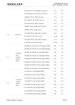
Страница 69: ... 1710 1784 9 1805 1879 9 MHz LTE B5 824 848 9 869 893 9 MHz LTE B7 2500 2569 9 2620 2689 9 MHz LTE B8 880 914 9 925 959 9 MHz LTE B20 832 861 9 791 820 9 MHz LTE B28 703 747 9 758 802 9 MHz LTE B38 2570 2619 9 2570 2619 9 MHz LTE B40 2300 2399 9 2300 2399 9 MHz LTE B41 2496 2689 9 2496 2689 9 MHz 3GPP Band Transmit Receive Unit WCDMA B2 1850 1910 1930 1990 MHz WCDMA B4 1710 1755 2110 2155 MHz WCDM...

Страница 70: ...2 R2 C3 C4 R3 C5 C6 R4 C7 C8 should be placed as close to the antennas as possible and are mounted according to the actual debugging C1 C8 are not mounted and a 0Ω resistor is mounted on R1 R4 respectively by default LTE B12 699 716 729 746 MHz LTE B13 777 787 746 756 MHz LTE B14 788 798 758 768 MHz LTE B17 704 716 734 746 MHz LTE B25 1850 1915 1930 1995 MHz LTE B26 814 849 859 894 MHz LTE B29 717...

Страница 71: ...eference Circuit of RF Antenna Interfaces Please keep a proper distance between the main antenna and the Rx diversity antenna to improve the receiving sensitivity 5 2 GNSS Antenna Interface 5 2 1 Pin Definition The following tables show pin definition and frequency specification of GNSS antenna interface Table 36 Pin Definition of GNSS Antenna Interface Pin Name Pin No I O Description Comment ANT_...

Страница 72: ...a VDD Module ANT_GNSS 47nH 10R 0 1uF 0R NM NM 100pF Figure 34 Reference Circuit of GNSS Antenna Interface 1 An external LDO can be selected to supply power according to the active antenna requirement 2 If the module is designed with a passive antenna then the VDD circuit is not needed Type Frequency Unit GPS 1575 42 1 023 MHz GLONASS 1597 5 1605 8 MHz Galileo 1575 42 2 046 MHz BeiDou 1561 098 2 04...

Страница 73: ...e trace width W the materials dielectric constant height from the reference ground to the signal layer H and the space between RF traces and grounds S Microstrip or coplanar waveguide is typically used in RF layout to control characteristic impedance The following are reference designs of microstrip or coplanar waveguide with different PCB structures Figure 35 Microstrip Design on a 2 layer PCB Fi...

Страница 74: ... to RF pins should not be designed as thermal relief pads and should be fully connected to ground The distance between the RF pins and the RF connector should be as short as possible and all the right angle traces should be changed to curved ones There should be clearance under the signal pin of the antenna connector or solder joint The reference ground of RF traces should be complete Meanwhile ad...

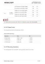
Страница 75: ...n 0dBi Active antenna noise figure 1 5dB Active antenna gain 0dBi Active antenna embedded LNA gain 17dB WCDMA LTE VSWR 2 Efficiency 30 Max Input Power 50W Input Impedance 50Ω Cable Insertion Loss 1dB WCDMA B5 B8 LTE B5 B8 B12 B13 B14 B17 B20 B26 B28 B29 B71 Cable Insertion Loss 1 5dB WCDMA B1 B2 B3 B4 LTE B1 B2 B3 B4 B25 B66 Cable Insertion Loss 2dB LTE B7 B38 B40 B41 B30 B42 B43 B48 1 It is recom...

Страница 76: ...allation If RF connector is used for antenna connection it is recommended to use the U FL R SMT connector provided by Hirose Figure 39 Dimensions of the U FL R SMT Connector Unit mm U FL LP serial connector listed in the following figure can be used to match the U FL R SMT Figure 40 Mechanicals of U FL LP Connectors ...

Страница 77: ...Series EG12 Hardware Design EG12_Hardware_Design 76 97 The following figure describes the space factor of mating plugs Figure 41 Space Factor of Mating Plugs Unit mm For more details please visit http www hirose com ...

Страница 78: ...ing table Table 39 Absolute Maximum Ratings 6 2 Power Supply Ratings Table 40 The Module s Power Supply Ratings Parameter Min Max Unit VBAT_RF VBAT_BB 0 3 4 7 V USB_VBUS 0 3 5 5 V Peak Current of VBAT_BB 0 1 0 A Peak Current of VBAT_RF 0 1 5 A Voltage at Digital Pins 0 3 2 3 V Voltage at ADC0 0 1 875 V Voltage at ADC1 0 1 875 V Parameter Description Conditions Min Typ Max Unit VBAT VBAT_BB and VBA...

Страница 79: ...l to be realized Only one or more parameters like Pout might reduce in their value and exceed the specified tolerances When the temperature returns to normal operating temperature levels the module will meet 3GPP specifications again 6 4 Current Consumption 6 4 1 EG12 GT Current Consumption Table 42 EG12 GT Current Consumption minimum and the maximum values USB_VBUS USB connection detection 3 3 5 ...

Страница 80: ...transfer GNSS OFF LTE TDD B42 CH42590 22 5dBm 350 mA LTE TDD B43 CH44590 22 5dBm 320 mA LTE TDD B48 CH55990 22 5dBm 320 mA Parameter Description Conditions Typ Unit IVBAT OFF state Power down 20 uA IVBAT Sleep state AT CFUN 0 USB disconnected 0 98 mA WCDMA PF 64 USB disconnected 2 51 mA WCDMA PF 128 USB disconnected 1 94 mA WCDMA PF 256 USB disconnected 1 62 mA WCDMA PF 512 USB disconnected 1 49 m...

Страница 81: ...B active 24 97 mA IVBAT WCDMA data transfer GNSS OFF WCDMA B1 HSDPA CH10700 22 93dBm 481 mA WCDMA B1 HSUPA CH10700 23 04dBm 477 mA WCDMA B3 HSDPA CH1338 22 9dBm 524 mA WCDMA B3 HSUPA CH1338 22 87dBm 540 mA WCDMA B5 HSDPA CH4407 23 19dBm 575 mA WCDMA B5 HSUPA CH4407 23 16dBm 573 mA WCDMA B8 HSDPA CH3012 23 25dBm 576 mA WCDMA B8 HSUPA CH3012 22 99dBm 577 mA IVBAT LTE data transfer GNSS OFF LTE FDD B...

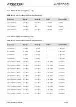
Страница 82: ...wer 6 6 RF Receiving Sensitivity The following tables show conducted RF receiving sensitivity of EG12 series module LTE TDD B40 CH39150 23 09dBm 353 mA LTE TDD B41 CH40620 22 79dBm 380 mA IVBAT WCDMA voice call WCDMA B1 CH10700 22 94dBm 475 mA WCDMA B3 CH1338 22 99dBm 524 mA WCDMA B5 CH4407 23 19dBm 562 mA WCDMA B8 CH3012 23 25dBm 577 mA Frequency Max Min WCDMA bands 24dBm 1 3dB 50dBm LTE FDD band...

Страница 83: ... 3GPP SIMO WCDMA B1 111dBm 111dBm 106 7dBm WCDMA B3 111dBm 111dBm 103 7dBm WCDMA B5 112dBm 112dBm 104 7dBm WCDMA B8 111dBm 112dBm 103 7dBm LTE FDD B1 10MHz 98 2dBm 98 7dBm 101 2dBm 96 3dBm LTE FDD B3 10MHz 98 7dBm 98 7dBm 101 7dBm 93 3dBm LTE FDD B5 10MHz 99 2dBm 99 4dBm 102 7dBm 94 3dBm LTE FDD B7 10MHz 97 7dBm 97 7dBm 100 2dBm 94 3dBm LTE FDD B8 10MHz 98 2dBm 98 5dBm 101 7dBm 93 3dBm LTE FDD B20...

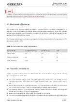
Страница 84: ...ics 6 8 Thermal Consideration In order to achieve better performance of the module it is recommended to comply with the following principles for thermal consideration On customers PCB design please keep placement of the module away from heating sources especially high power components such as ARM processor audio power amplifier power supply etc Do not place components on the opposite side of the P...

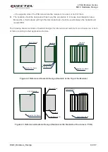
Страница 85: ...he heatsink and module PCB The following shows two kinds of heatsink designs for reference and customers can choose one or both of them according to their application structure Heatsink EG12 Module Application Board Application Board Heatsink Thermal Pad Shielding Cover Figure 42 Referenced Heatsink Design Heatsink at the Top of the Module Thermal Pad Heatsink Application Board Application Board H...

Страница 86: ...ling may be required depending on the integrated application 2 In order to protect the components from damage the thermal design should be maximally optimized to guarantee that the module s internal temperature always maintains below 105 C Customers can execute AT QTEMP command to get the module s internal temperature 3 For more detailed guidelines on thermal design please refer to document 7 NOTE...

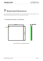
Страница 87: ...echanical Dimensions This chapter describes the mechanical dimensions of the module All dimensions are measured in mm and the dimensional tolerances are 0 05mm unless otherwise specified 7 1 Mechanical Dimensions of the Module Pin1 Figure 44 Module Top and Side Dimensions ...

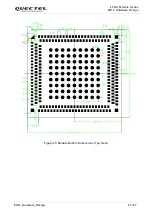
Страница 88: ...LTE A Module Series EG12 Hardware Design EG12_Hardware_Design 87 97 Figure 45 Module Bottom Dimensions Top View ...

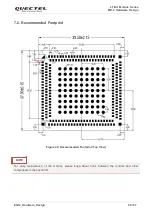
Страница 89: ...Hardware Design EG12_Hardware_Design 88 97 7 2 Recommended Footprint Figure 46 Recommended Footprint Top View For easy maintenance of the module please keep about 3mm between the module and other components in the host PCB NOTE ...

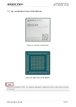
Страница 90: ..._Hardware_Design 89 97 7 3 Top and Bottom Views of the Module Figure 47 Top View of the Module Figure 48 Bottom View of the Module These are renderings of EG12 For authentic appearance please refer to the module that you receive from Quectel NOTE ...

Страница 91: ...ctory environment of 30º C 60 RH Stored at 10 RH 3 Devices require baking before mounting if any circumstance below occurs When the ambient temperature is 23º C 5º C and the humidity indicator card shows the humidity is 10 before opening the vacuum sealed bag Device mounting cannot be finished within 168 hours at factory conditions of 30º C 60 RH 4 If baking is required devices may be baked for 8 ...

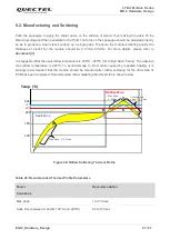
Страница 92: ... is suggested that the peak reflow temperature is 238º C 245º C for SnAg3 0Cu0 5 alloy The absolute max reflow temperature is 245º C To avoid damage to the module caused by repeated heating it is strongly recommended that the module should be mounted after reflow soldering for the other side of PCB has been completed Recommended reflow soldering thermal profile is shown below Temp C Reflow Zone So...

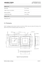
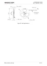
Страница 93: ...l carriers Each reel is 10 56m long and contains 200 modules The figures below show the packaging details measured in mm Figure 50 Tape Specifications Reflow Zone Max slope 2 to 3 C sec Reflow time D over 220 C 40 to 60 sec Max temperature 238 C 245 C Cooling down slope 1 to 4 C sec Reflow Cycle Max reflow cycle 1 ...

Страница 94: ...LTE A Module Series EG12 Hardware Design EG12_Hardware_Design 93 97 Figure 51 Reel Specifications ...

Страница 95: ...S Application Note for EM12 EG12 and EG18 4 Quectel_Module_Secondary_SMT_User_Guide Module Secondary SMT User Guide 5 Quectel_EG12 EG18_Reference_Design Reference Design for EG12 and EG18 6 Quectel_RF_Layout_Application_Note RF Layout Application Note 7 Quectel_LTE_Module_Thermal_Design_Guide Thermal Design Guide for LTE Modules 8 Quectel_EG12_CA_Feature EG12 CA Feature Abbreviation Description AM...

Страница 96: ...NASS GLObalnaya NAvigatsionnaya Sputnikovaya Sistema the Russian Global Navigation Satellite System GMSK Gaussian Minimum Shift Keying GNSS Global Navigation Satellite System GPS Global Positioning System HO RXD Higher order Receiver Diversity HR Half Rate I O Input Output Inorm Normal Current LED Light Emitting Diode LNA Low Noise Amplifier LTE Long Term Evolution MIMO Multiple Input Multiple Out...

Страница 97: ...abit Media Independent Interface SIMO Single Input Multiple Output SMS Short Message Service TDD Time Division Duplexing Tx Transmitting Direction UL Uplink UMTS Universal Mobile Telecommunications System URC Unsolicited Result Code U SIM Universal Subscriber Identity Module Vmax Maximum Voltage Value Vnorm Normal Voltage Value Vmin Minimum Voltage Value VIHmax Maximum Input High Level Voltage Val...

Страница 98: ...ximum Input Voltage Value VImin Absolute Minimum Input Voltage Value VOHmax Maximum Output High Level Voltage Value VOHmin Minimum Output High Level Voltage Value VOLmax Maximum Output Low Level Voltage Value VOLmin Minimum Output Low Level Voltage Value VSWR Voltage Standing Wave Ratio ...

Отзывы: