background image


GSM/GPRS/NB-IoT  Module  Series 

                                                                            BC68&M66  Compatible  Design


BC68&M66_Compatible_Design                                                                                                                21 / 31 


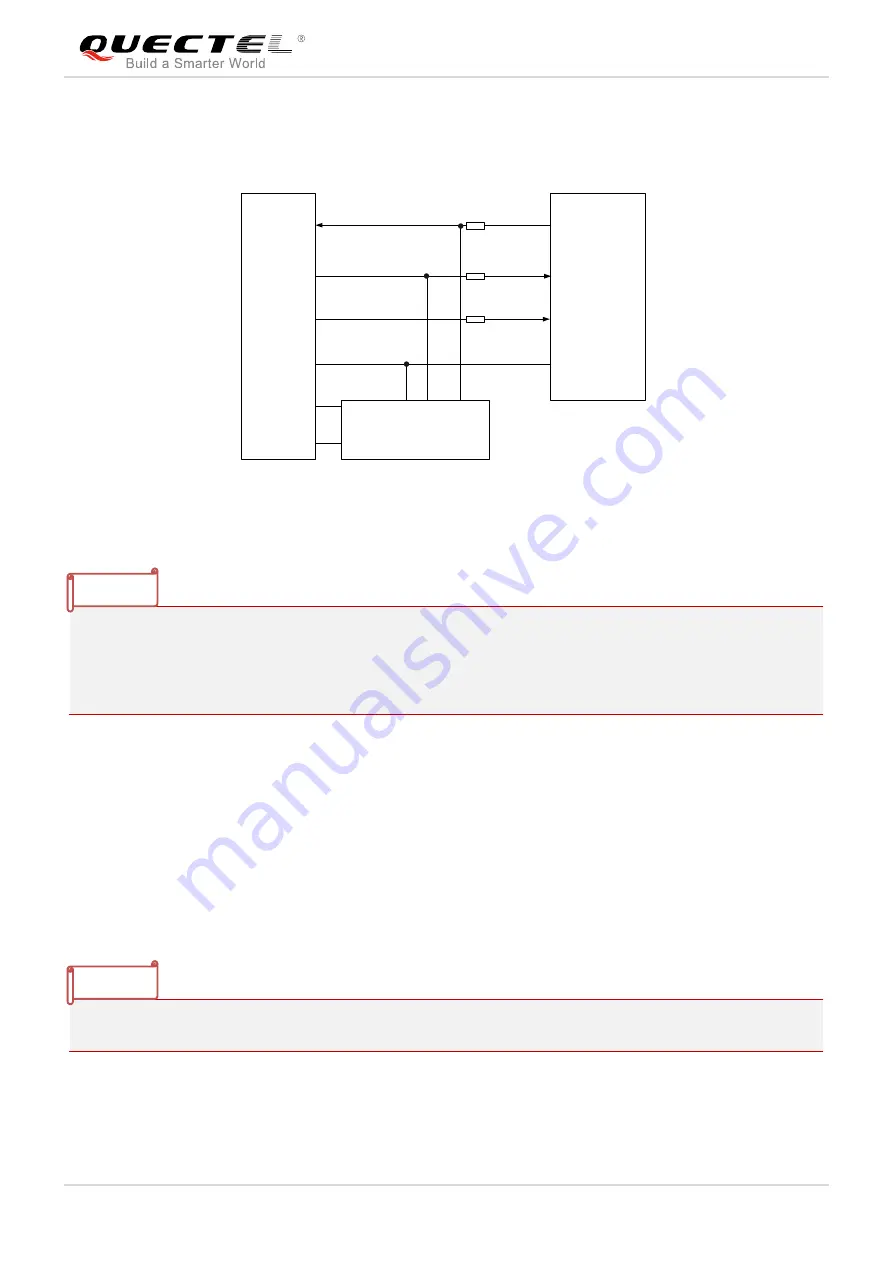
If the DTE is 3.0V or 3.3V power domain, a reference design of 3.3V level match for BC68 is shown as 

below. 

DTE

TXD

RXD

1K

TXD

RXD

RI

RI

BC68

Voltage level: 3.3V

1K

1K

GND

GND

TXD RXD

GND

TEST POINTS

RESET

VBAT

VBAT

RESET


Figure 13: Reference Design of BC68 UART Interface for 3.3V System 


1.  In order to reduce the power consumption of the system, it is highly recommended to add resistors 

with resistance greater than 1KΩ on the UART port signal traces when the host’s voltage level is 3.0V 
or 3.3V.   

2.  It is recommended to reserve the test points (RXD, TXD, RESET and VBAT) for firmware upgrading. 


4.8. ADC Interface 


The pin ADC* of BC68 module and the pin ADC0 of M66 provide a 10-bit ADC input channel to read the 

voltage value. In addition, M66 offers an AVDD pin to provide a reference voltage for ADC0 and the max 

voltage  of  AVDD  is  2.8V.  In  order  to  improve  the  accuracy  of  ADC,  the  layout  of  ADC  should  be 

surrounded by ground. 


“*” means under development. 


NOTES 

NOTE 


Содержание BC68

Страница 1: ...BC68 M66 Compatible Design NB IoT GSM GPRS Module Series Rev BC68 M66_Compatible_Design_V1 0 Date 2018 03 22 Status Released www quectel com...

Страница 2: ...MATION PROVIDED IS BASED UPON CUSTOMERS REQUIREMENTS QUECTEL MAKES EVERY EFFORT TO ENSURE THE QUALITY OF THE INFORMATION IT MAKES AVAILABLE QUECTEL DOES NOT MAKE ANY WARRANTY AS TO THE INFORMATION CON...

Страница 3: ...GSM GPRS NB IoT Module Series BC68 M66 Compatible Design BC68 M66_Compatible_Design 2 31 About the Document History Revision Date Author Description 1 0 2018 03 22 Power JIN Initial...

Страница 4: ...4 4 1 2 Reduce Voltage Drop 14 4 2 Power on Circuit 15 4 3 Power off Circuit 16 4 3 1 Power down Module via AT Command 16 4 3 2 Power down M66 Using PWRKEY Pin 17 4 4 Reset BC68 18 4 5 Network Status...

Страница 5: ...Design 4 31 Table Index TABLE 1 MODULE GENERAL INFORMATION 7 TABLE 2 FEATURES OVERVIEW 8 TABLE 3 I O PARAMETERS DEFINITION 11 TABLE 4 PIN COMPARISON BETWEEN BC68 AND M66 11 TABLE 5 UART INTERFACE VOLT...

Страница 6: ...NG OF RESETTING MODULE 18 FIGURE 10 REFERENCE CIRCUIT OF NETLIGHT 19 FIGURE 11 REFERENCE CIRCUIT OF U SIM CARD INTERFACE WITH A 6 PIN U SIM CARD CONNECTOR 19 FIGURE 12 REFERENCE DESIGN OF M66 UART INT...

Страница 7: ...ompatible Design BC68 M66_Compatible_Design 6 31 1 Introduction Quectel BC68 is a high performance NB IoT module compatible with Quectel GSM GPRS M66 module This document briefly describes the compati...

Страница 8: ...emes CS 1 CS 2 CS 3 and CS 4 BC68 is a high performance NB IoT module with low power consumption BC68 and M66 are designed as compatible products Customers can choose a proper module according to spec...

Страница 9: ...ot supported Multi slot class 12 BT Not supported Supported BT3 0 Temperature Range Operation temperature range 35 C 75 C 1 Extended temperature range 40 C 85 C 2 Storage temperature range 40 C 90 C O...

Страница 10: ...unrecoverable malfunction There are also no effects on radio spectrum and no harm to radio network Only one or more parameters like Pout might reduce in their value and exceed the specified tolerances...

Страница 11: ...BC68 M66 RESERVED RESERVED RESERVED RESERVED RESERVED RESERVED RESERVED RESERVED RESERVED RESERVED RESERVED RESERVED RESERVED RESERVED 45 46 47 48 49 50 51 52 53 54 55 56 57 58 BC68 M66 Top View AGND...

Страница 12: ...s between BC68 and M66 Table 4 Pin Comparison between BC68 and M66 Symbol Description IO Bidirectional DI Digital Input DO Digital Output PI Power Input PO Power Output AI Analog Input AO Analog Outpu...

Страница 13: ...SIM card reset signal 13 SIM_CLK DO USIM clock SIM_CLK DO U SIM card clock signal 14 SIM_VDD PO Power supply for USIM card SIM_VDD PO Power supply for U SIM card 15 RESET DI Reset the module RESERVED...

Страница 14: ...VED RXD_AUX DI Receive data 29 RESERVED TXD_AUX DO Transmit data 30 RESERVED PCM_CLK DO PCM clock 31 RESERVED PCM_SYNC DO PCM frame synchronization 32 RESERVED PCM_IN DI PCM data input 33 RESERVED PCM...

Страница 15: ...added on the VBAT trace to increase surge voltage withstand capability The following figure shows a reference design for battery power supply and the designed output of the power supply is about 3 6V...

Страница 16: ...turn on method of BC68 is different from M66 BC68 can be powered on automatically when VBAT pins are powered M66 will be powered on by driving the pin PWRKEY to a low level voltage for more than 100m...

Страница 17: ...always pull down PWRKEY pin 2 The parts marked in green in the above figure are for BC68 3 The parts marked in black in the above figure are for M66 4 3 Power off Circuit 4 3 1 Power down Module via...

Страница 18: ...ts marked in black in the above figure are for M66 3 The time for the module to log out from network depends on local network quality 4 3 2 Power down M66 Using PWRKEY Pin It is a safe way to turn off...

Страница 19: ...ore than 100ms The reset scenario for BC68 by RESET is illustrated in the figure below 4 7K 47K pulse BC68 RESET 100ms 100ms Figure 8 Reference Circuit of RESET by Using Driving Circuit The reset scen...

Страница 20: ...erface M66 supports 1 8V or 3 0V SIM USIM cards while BC68 supports 1 8V or 3 0V USIM cards The pin assignment of BC68 s USIM interface and M66 s U SIM interface is compatible The following figure sho...

Страница 21: ...recommended to add a level match circuit between the module and the DTE because of the different power domain of their UART interface For details please refer to document 4 DCD B RI B CTS B TXD B DCD...

Страница 22: ...the system it is highly recommended to add resistors with resistance greater than 1K on the UART port signal traces when the host s voltage level is 3 0V or 3 3V 2 It is recommended to reserve the te...

Страница 23: ...ce of 50 A reference circuit for the interface is shown below In order to achieve better RF performance a type matching circuit should be reserved and the type matching components R1 C1 C2 should be p...

Страница 24: ...31 5 Recommended Footprint and Stencil Design This chapter mainly introduces the recommended footprint and stencil design for BC68 and M66 modules 5 1 Recommended Compatible Footprint The following f...

Страница 25: ...BC68 M66 Unit mm 1 The modules should be kept about 3mm away from other components in the host PCB 2 The circular test points with a radius of 1 4mm in the above recommended footprint should not be d...

Страница 26: ...n The thickness of PCB is different In order to ensure the module soldering quality the thickness of stencil is recommended to be 0 2mm for M66 and 0 18mm for BC68 For more details please refer to doc...

Страница 27: ...GSM GPRS NB IoT Module Series BC68 M66 Compatible Design BC68 M66_Compatible_Design 26 31 The recommended stencil design for M66 is shown as below Figure 18 Recommended Stencil Design for M66 Unit mm...

Страница 28: ...le Series BC68 M66 Compatible Design BC68 M66_Compatible_Design 27 31 5 3 Installation Sketch Map The following figure shows the sketch map of installation for BC68 and M66 Figure 19 Installation Sket...

Страница 29: ...e on a single pass It is suggested that the peak reflow temperature is 235 C 245 C for SnAg3 0Cu0 5 alloy The absolute max reflow temperature is 260 C To avoid damage to the module caused by repeated...

Страница 30: ...he modules are stored inside a vacuum sealed bag which is ESD protected It should not be opened until the devices are ready to be soldered onto the application 6 2 1 BC68 and M66 Packaging The reel is...

Страница 31: ...Manual for BC68 and BC95 G 3 Quectel_BC68_Hardware_Design BC68 Hardware Design 4 Quectel_M66_Hardware_Design M66 Hardware Design 5 Module_Secondary_SMT_User_Guide Module Secondary SMT User Guide Abbr...

Страница 32: ...nd Grid Array LTE Long Term Evolution NB IoT Narrow Band Internet of Things PCB Printed Circuit Board PCM Pulse Code Modulation PCS Personal Communication System PSM Power Saving Mode RF Radio Frequen...

Отзывы:

Похожие инструкции для BC68