background image


      NB-IoT  Module  Series 

                                                                                                                                BC66  Hardware  Design


BC66_Hardware_Design                                                                                                                              24 / 57 


3.7.3.  Reset the Module 

Driving the RESET pin to a low level voltage for at least 50ms will reset the module.   


Table 8: Reset Pin 

Pin Name   

Pin No. 

Description 

Reset Pull-down Time 

RESET 

15 

Reset the module.   

Active low. 

50ms 


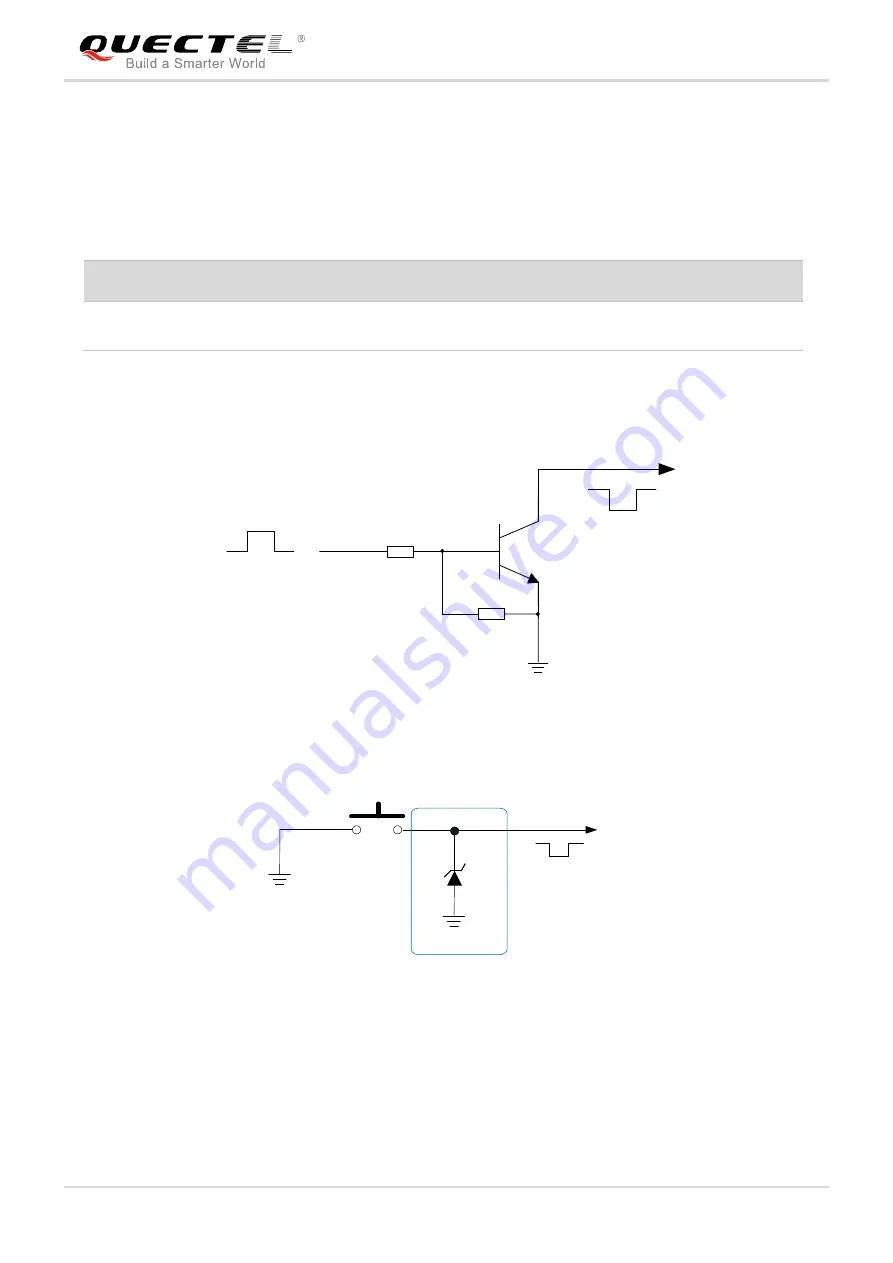
The recommended circuits of resetting the module are shown below. An open drain/collector driver or 

button can be used to control the RESET pin. 


Reset pulse

RESET

4.7K

47K


Figure 11: Reference Circuit of RESET by Using Driving Circuit 


RESET

S1

Close to S1

TVS


Figure 12: Reference Circuit of RESET by Using Button 


The reset scenario is illustrated in the following figure. 

Содержание BC66

Страница 1: ...BC66 Hardware Design NB IoT Module Series Rev BC66_Hardware_Design_V1 1 Date 2018 11 14 Status Released www quectel com...

Страница 2: ...PROVIDED IS BASED UPON CUSTOMERS REQUIREMENTS QUECTEL MAKES EVERY EFFORT TO ENSURE THE QUALITY OF THE INFORMATION IT MAKES AVAILABLE QUECTEL DOES NOT MAKE ANY WARRANTY AS TO THE INFORMATION CONTAINED...

Страница 3: ...dware Design BC66_Hardware_Design 2 57 About the Document History Revision Date Author Description 1 0 2018 08 24 Speed SUN Newgate HUA Initial 1 1 2018 11 14 Newgate HUA Updated supported bands and i...

Страница 4: ...s 18 3 5 Power Saving Mode PSM 19 3 6 Power Supply 20 3 6 1 Power Supply Pins 20 3 6 2 Reference Design for Power Supply 21 3 7 Power up Power down Scenarios 21 3 7 1 Turn on 21 3 7 2 Turn off 23 3 7...

Страница 5: ...lity Characteristics 43 5 1 Operation and Storage Temperatures 43 5 2 Current Consumption 43 5 3 Electrostatic Discharge 45 6 Mechanical Dimensions 47 6 1 Mechanical Dimensions of the Module 47 6 2 Re...

Страница 6: ...ON OF USIM INTERFACE 31 TABLE 12 PIN DEFINITION OF ADC INTERFACE 32 TABLE 13 PIN DEFINITION OF NB IOT ANTENNA INTERFACE 34 TABLE 14 MODULE OPERATING FREQUENCIES 34 TABLE 15 ANTENNA CABLE INSERTION LOS...

Страница 7: ...T 27 FIGURE 17 REFERENCE CIRCUIT WITH VOLTAGE LEVEL TRANSLATOR CHIP 28 FIGURE 18 REFERENCE CIRCUIT WITH TRANSISTOR CIRCUIT 28 FIGURE 19 SKETCH MAP FOR RS 232 INTERFACE MATCH 29 FIGURE 20 SPI INTERFACE...

Страница 8: ...rdware interface which are connected with the customers applications This document can help customers quickly understand module interface specifications electrical and mechanical details as well as ot...

Страница 9: ...nsult the airline staff for more restrictions on the use of wireless devices on boarding the aircraft Wireless devices may cause interference on sensitive medical equipment so please be aware of the r...

Страница 10: ...ide reliable connectivity with the applications BC66 provides abundant external interfaces UART SPI ADC NETLIGHT etc and protocol stacks UDP TCP LwM2M MQTT etc which provide great convenience for cust...

Страница 11: ...ing on the module the MCU has to send AT command consecutively to synchronize baud rate with the module When OK is returned it indicates the baud rate has been synchronized successfully When the modul...

Страница 12: ...the temperature returns to normal operation temperature levels the module will meet 3GPP specifications again 3 means under development 2 3 Functional Diagram The following figure shows a block diagr...

Страница 13: ...RX 32KHz RTC BLOCK LDO PSM_EINT USIM Enable PWRKEY DBG_UART USIM SPI VBAT VDD_EXT ASM Figure 1 Functional Diagram means under development 2 4 Development Board Quectel provides a complete set of devel...

Страница 14: ...pped with a total of 58 pins including 44 LCC pins and 14 LGA pins The subsequent chapters will provide detailed descriptions of the following functions pins interfaces PSM Power Supply RESET PWRKEY U...

Страница 15: ...ESERVED RESERVED TXD_AUX RXD_AUX GND RESERVED RESERVED VDD_EXT RESERVED RESERVED RI PSM_EINT RXD TXD NETLIGHT RESET SIM_VDD VBAT_RF POWER GND UART USIM ANT RESERVED 45 46 47 48 49 50 51 52 53 54 55 56...

Страница 16: ...ly Pin Name Pin No I O Description DC Characteristics Comment VBAT_BB 42 PI Power supply for the module s baseband part Vmax 3 63V Vmin 2 1V Vnorm 3 3V VBAT_RF 43 PI Power supply for the module s RF p...

Страница 17: ...n No I O Description DC Characteristics Comment PSM_EINT 19 DI Dedicated external interrupt pin Used to wake up the module from PSM Network Status Indication Pin Name Pin No I O Description DC Charact...

Страница 18: ...domain USIM Interface Pin Name Pin No I O Description DC Characteristics Comment SIM_VDD 14 DO USIM card power supply Vnorm 1 8V SIM_RST 12 DO USIM card reset signal VOLmax 0 15 SIM_VDD VOHmin 0 85 SI...

Страница 19: ...eep all unused pins unconnected 2 means under development 3 4 Operating Modes The following table briefly describes the three operating modes of the module Table 5 Overview of Operating Modes Mode Fun...

Страница 20: ...e module and the mobile reachable timer starts When the T3324 timer expires the module enters PSM for duration of T3412 periodic TAU timer Please note that the module cannot request PSM when it is est...

Страница 21: ...The module cannot be woken up by any other general purpose GPIO interrupts 3 6 Power Supply 3 6 1 Power Supply Pins BC66 provides two VBAT pins for connection with an external power supply The table...

Страница 22: ...o place a 100uF tantalum capacitor with low ESR ESR 0 7 and three ceramic capacitors 100nF 100pF and 22pF near the VBAT pins Also it is recommended to add a TVS diode on the VBAT trace near VBAT pins...

Страница 23: ...her way to control the PWRKEY is using a button directly When pressing the key electrostatic strike may generate from the finger Therefore a TVS component is indispensable to be placed nearby the butt...

Страница 24: ...following methods Power off by AT QPOWD 0 In emergent conditions the module can be powered off through disconnecting VBAT power supply The module will be powered off automatically when VBAT drops bel...

Страница 25: ...t Pull down Time RESET 15 Reset the module Active low 50ms The recommended circuits of resetting the module are shown below An open drain collector driver or button can be used to control the RESET pi...

Страница 26: ...e traditional DCE DTE Data Terminal Equipment connection Table 9 Pin Definition of UART Interfaces Interface Pin Name Pin No Description Comment Main UART Port TXD 17 Send data to RXD of DTE 1 8V powe...

Страница 27: ...urned it indicates the baud rate has been synchronized successfully When the module is woken up from PSM or idle mode the baud rate synchronized during start up will be used directly When the port is...

Страница 28: ...re flow control Its baud rate is 115200bps by default The following is a reference design of auxiliary UART port DTE TXD RXD GND Module TXD_AUX RXD_AUX GND Figure 16 Reference Design of Auxiliary UART...

Страница 29: ...rcuit design of dotted line section can refer to the design of solid line section in terms of both module input and output circuit designs but please pay attention to the direction of connection DTE V...

Страница 30: ...h Please visit vendors websites to select a suitable RS 232 transceiver such as http www exar com and http www maximintegrated com 1 Transistor circuit solution is not suitable for applications with h...

Страница 31: ...SPI MOSI_SPI 0 1uF 0 1uF CS_SPI SCLK_SPI MISO_SPI MOSI_SPI VDD Translator Module DTE MISO_SPI Figure 20 SPI Interface Reference Circuit with Translator Chip 3 10 USIM Interface The module provides a U...

Страница 32: ...nt of USIM card connector as close as possible to the module Keep the trace length as less than 200mm as possible Keep USIM card signals away from RF and VBAT traces Assure the trace between the groun...

Страница 33: ...that the USIM peripheral circuit should be close to the USIM card connector Place the RF bypass capacitors 33pF close to the USIM card connector on all signal traces to improve EMI suppression 3 11 A...

Страница 34: ...NB IoT Module Series BC66 Hardware Design BC66_Hardware_Design 33 57 Module NETLIGHT 4 7K 47K 2 2K VBAT Figure 22 Reference Design for NETLIGHT means under development NOTE...

Страница 35: ...2 Operating Frequencies Table 14 Module Operating Frequencies Pin Name Pin No Description RF_ANT 35 RF antenna interface GND 34 36 37 Ground Frequency Band Receiving Frequency Transmitting Frequency...

Страница 36: ...ntenna pad in order to give a better grounding In order to achieve better RF performance it is recommended to reserve a type matching circuit and place the type matching components R1 C1 C2 as close t...

Страница 37: ...es should be controlled as 50 The impedance of the RF traces is usually determined by the trace width W the materials dielectric constant the height between signal layer and reference ground H and the...

Страница 38: ...on a 2 layer PCB Figure 26 Coplanar Waveguide Line Design on a 4 layer PCB Layer 3 as Reference Ground Figure 27 Coplanar Waveguide Line Design on a 4 layer PCB Layer 4 as Reference Ground In order t...

Страница 39: ...ng some ground vias around RF traces and the reference ground could help to improve RF performance The distance between the ground vias and RF traces should be no less than two times the width of RF s...

Страница 40: ...s in 3GPP Rel 13 and 3GPP Rel 14 2 means under development Frequency Band Max Min B1 23dBm 2dB 39dBm B2 23dBm 2dB 39dBm B3 23dBm 2dB 39dBm B4 23dBm 2dB 39dBm B5 23dBm 2dB 39dBm B8 23dBm 2dB 39dBm B12...

Страница 41: ...vity Table 18 Receiving Sensitivity with RF Retransmissions means under development Frequency Band Receiving Sensitivity B1 129dBm B2 129dBm B3 129dBm B4 129dBm B5 129dBm B8 129dBm B12 129dBm B13 129d...

Страница 42: ...lation If RF connector is used for antenna connection it is recommended to use the U FL R SMT connector provided by HIROSE Figure 28 Dimensions of the U FL R SMT Connector Unit mm U FL LP serial conne...

Страница 43: ...es BC66 Hardware Design BC66_Hardware_Design 42 57 The following figure describes the space factor of mated connector Figure 30 Space Factor of Mated Connector Unit mm For more details please visit ht...

Страница 44: ...h and maintain an SMS data transmission etc There is no unrecoverable malfunction There are also no effects on radio spectrum and no harm to radio network Only one or more parameters like Pout might r...

Страница 45: ...tone 15kHz subcarrier spacing B1 23dBm 100 285 mA B2 23dBm 103 294 mA B3 23dBm 107 308 mA B4 23dBm TBD TBD mA B5 23dBm 107 303 mA B8 23dBm 113 325 mA B12 23dBm 134 393 mA B13 23dBm 111 319 mA B17 23d...

Страница 46: ...mA B66 23dBm 200 316 mA 1 1 Current consumption under instrument test condition 2 means under development 5 3 Electrostatic Discharge The module is not protected against electrostatics discharge ESD...

Страница 47: ...ardware Design BC66_Hardware_Design 46 57 Table 21 Electrostatic Discharge Characteristics 25 C 45 Relative Humidity Test Contact Discharge Air Discharge Unit VBAT GND 5 10 kV Antenna interface 5 10 k...

Страница 48: ...al Dimensions This chapter describes the mechanical dimensions of the module All dimensions are measured in millimetre mm and the tolerances for dimensions without tolerance values are 0 05mm 6 1 Mech...

Страница 49: ...NB IoT Module Series BC66 Hardware Design BC66_Hardware_Design 48 57 Figure 32 Module Bottom Dimension Bottom View...

Страница 50: ...dule Series BC66 Hardware Design BC66_Hardware_Design 49 57 6 2 Recommended Footprint Figure 33 Recommended Footprint Unit mm The module should be kept about 3mm away from other components on the host...

Страница 51: ...esign 50 57 6 3 Top and Bottom Views of the Module Figure 31 Top View of the Module Figure 32 Bottom View of the Module These are renderings of BC66 module For authentic dimension and appearance pleas...

Страница 52: ...at the factory environment of 30 C 60 RH Stored at 10 RH 3 Devices require baking before mounting if any circumstance below occurs When the ambient temperature is 23 C 5 C and the humidity indication...

Страница 53: ...the peak reflow temperature is 240 245 C and the absolute maximum reflow temperature is 245 C To avoid damage to the module caused by repeated heating it is strongly recommended that the module shoul...

Страница 54: ...fter 12 hours Neutral Salt Spray test the laser engraved label information on the shielding can is still clearly identifiable and the QR code is still readable although white rust may be found 7 3 Pac...

Страница 55: ...NB IoT Module Series BC66 Hardware Design BC66_Hardware_Design 54 57 Figure 33 Tape Dimensions Unit mm Figure 34 Reel Dimensions Unit mm...

Страница 56: ...el_Module_Secondary_SMT_User_Guide Module Secondary SMT User Guide Abbreviation Description ADC Analog to Digital Converter CoAP Constrained Application Protocol DCE Data Communications Equipment typi...

Страница 57: ...ternet of Things PCB Printed Circuit Board PDU Protocol Data Unit PPP Point to Point Protocol PSM Power Save Mode RF Radio Frequency RTC Real Time Clock RXD Receive Data SMS Short Message Service SSL...

Страница 58: ...evel Voltage Value VILmax Maximum Input Low Level Voltage Value VILmin Minimum Input Low Level Voltage Value VImax Absolute Maximum Input Voltage Value VInorm Absolute Normal Input Voltage Value VImin...

Отзывы: