


3
Connections
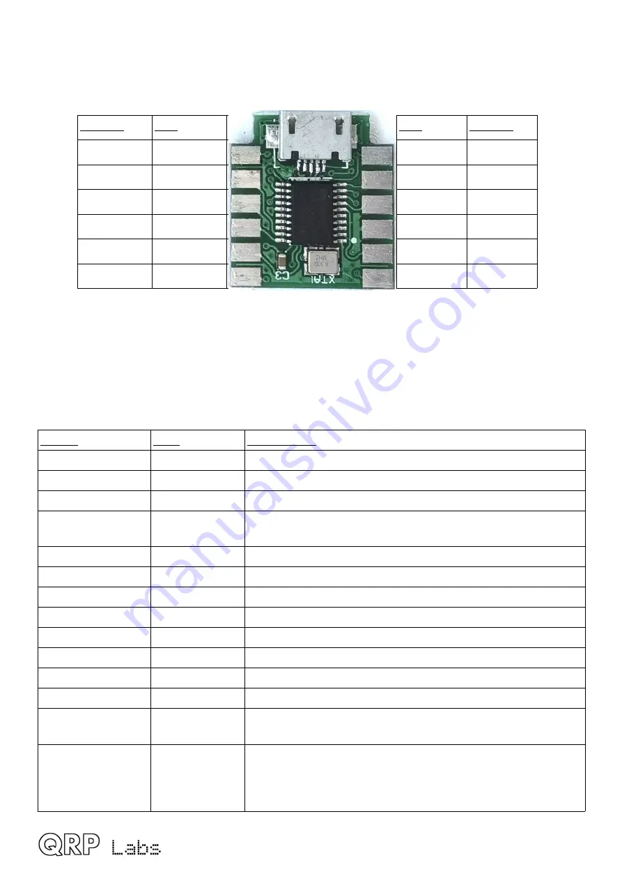
This table shows the pinout of the ProgRock2 module:
Bottom
Top
Top
Bottom
13. USB -
1. USB +
12. V+
24. CLK 2
14. SCL
2. SWDIO
11.BANK 2 23. CLK 1
15. SDA
3. GND
10.BANK 1 22. RXD
16. 1 PPS
4. SWCLK
9. GND
21. TXD
17. +3V3
5. BANK 2
8. BANK 0 20. GND
18. GND
6. V+
7. CLK 0
19. GND
You will note that there is a row of 6 pads along each long edge of the PCB, on top and bottom
sides, making a total of 24 possible connections. Some, such as GND, are on multiple pads. For
convenience these are labeled 1 to 24. In the diagram above, the pads on the top side are shown
closest to the PCB pads, and the bottom side pads are the outer table column.
The layout was carefully designed to allow as much future flexibility as possible.
The signals are as follows:
Signal
Pins
Description
GND
3, 9, 18, 19, 20 Ground.
V+
6, 12
Positive supply voltage.
+3V3
17
3.3V output from onboard voltage regulator.
USB-, USB+
13, 1
USB port (also connected to micro-USB connector); note,
also sometimes called USB_DM, USB_DP respectively.
SWDIO, SWCLK
2, 4
Chip programming pins: Factory use only.
SCL, SDA
14, 15
I2C serial bus (internal use only, currently).
RXD, TXD
22, 21
USART port (unused currently).
BANK 0
8
Bank select input 0 (3.3V max).
BANK 1
10
Bank select input 1 (3.3V max).
BANK 2
5, 11
Bank select input 2 (3.3V max).
CLK 0
7
Si5351A Clock 0 output.
CLK 1
23
Si5351A Clock 1 output.
CLK 2
24
Si5351A Clock 2 output (not available when using GPS
discipline).
1 PPS
16
1 PPS input, connect to 1pps output of GPS for GPS
discipline. Note that the signal requires 3.3V. If using a 5V
GPS output, use a 3.9K series resistor (value not critical;
3.9K was used during testing).
ProgRock2 manual 1.00b
5


