Power Application Controller
®
-30-
Copyright 2020 © Qorvo, Inc.
Rev 1.2
– Jan 17, 2019
8.3
System Block Diagram
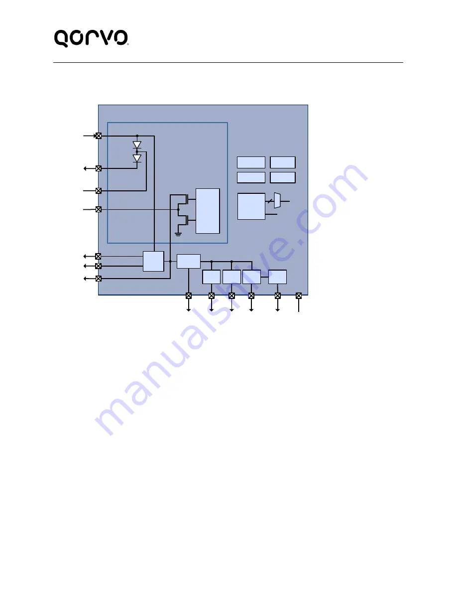
Figure 8-1 Power Manager System Block Diagram
POWER MANAGER
VM
VP
LI NEAR
REG
VCCIO
VCORE VCC33
TIMERS
HIBERNATE
2. 5/3.0V
V
REF
V
THREF
PO WER
& TEMP
MON
V
MON
V
TEMP
CHARGE PUMP
M
U
X
MVBB
SW1
VCP
CPH
CPL
CHARGE
PUMP
CONTRO L
LI NEAR
REG
VSYS
VSS
SW2
LI NEAR
REG
LI NEAR
REG
LI NEAR
REG
VCC18
8.4
Functional Description
The Power Manager is optimized to efficiently provide “all-in-one” power management required
by the PAC and associated application circuitry. It incorporates a High-Voltage charge pump
(HVCP) DC/DC to generate the supply for the integrated high-side gate drivers and a Medium-
Voltage Buck-Boost Converter (MVBB) to generate the supply for the integrated low-side gate
drivers.
Five additional linear regulators provide V
SYS
, V
CCIO
, V
CC33
, V
CC18
and V
CORE
supplies for 5V
system, 3.3V I/O, 3.3V mixed signal, MCU FLASH and 1.2V microcontroller core circuitry. The
power manager also handles system functions including internal reference generation, timers,
hibernate mode management, and power and temperature monitoring.
8.5
VP Low Warning
If the VP low-side gate driver supply (output of the MVBB) is below the power good state, then
the following actions are taken:
•
SOC.STATUS.VPLOW
is set to 1b
•
SOC.STATUS.VPLOW_LATCH
is set to 1b
•
If the
SOC.FAULTEN.nVPFLT
bit is set to 1b, the IRQ1 interrupt to the MCU is asserted


