


BIOS Setup Information
PCOM-
B630VG User’s Manual
Chapter 2
Hardware Configuration
This chapter indicates connectors’ Pin Assignment.
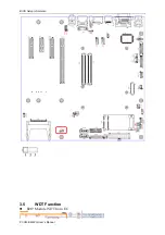
2.1
Connector Allocation
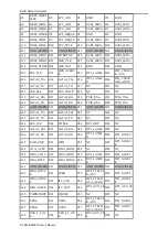
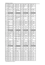
Connector Function List
Connector
Function
Remark
J1
DDR3 channel A connector.
J2
DDR3 channel B connector.
J3
COM Express connector raw C and D
J4
COM Express connector raw A and B
Pin Assignment of Connectors
J3
J4
Row A
Row B
Row C
Row D
Pin
No
Signal
Description
Pin
No
Signal
Description
Pin
No
Signal
Description
Pin
No
Signal
Description
A1
GND (FIXED) B1
GND (FIXED) C1
GND (FIXED) D1
GND (FIXED)
A2
GBE0_MDI3- B2
GBE0_ACT# C2
GND
D2
GND
A3
GB B3
LPC_FRAME
#
C3
USB0_SSRX- D3
USB0_SSTX-
A4
GBE0_LINK1
00#
B4
LPC_AD0
C4
US D4
US
J1
J2
J3
J4
Содержание PCOM-B630VG
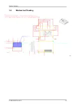
Страница 6: ...System Overview PCOM B219VG VI ECC 1 3 1 4 Mechanical Drawing ...
Страница 7: ...System Overview PCOM B219VG VI ECC 1 4 1 5 System Architecture ...
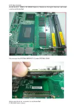
Страница 18: ...BIOS Setup Information PCOM B630VG User s Manual 3 5 WDT Function B219 Module WDT from EC ...
Страница 32: ...Troubleshooting PCOM B630VG User s Manual Panel Color Depth 18Bit Default 24Bir ...
Страница 41: ...Troubleshooting PCOM B630VG User s Manual Super IO Configuration ...


