PMC-990996 (R2)
PROPRIETARY AND CONFIDENTIAL TO PMC-SIERRA, INC., AND FOR ITS CUSTOMERS’ INTERNAL USE
ã
1999 PMC-Sierra, Inc.
PM7347
PMC-Sierra,Inc.
SATURN User Network Interface for J2/E3/T3
S/UNI-JET
FEATURES
• Single-chip ATM User Network
Interface (UNI) operating at 44.736
Mbit/s, 34.368 Mbit/s, and 6.312 Mbit/s
conforming to ATMF-95-1207R1,
ATMF-94-0406R5, and
AF-PHY-0029.000.
• Provides on-chip DS3, E3 (G.751 and
G.832), and J2 framers. Can be
configured for use solely as a framer.
When configured in framer mode,
gapped transmit and receive clocks
can be generated for interfaces that
need access only to payload data bits.
• Supports bypass of the internal
framers and supports connections to
an arbitrary-rate external transmission
system interface up to a rate of 52
Mbit/s. This lets the S/UNI-JET be
used as an ATM cell delineator.
• Implements ATM direct-cell mapping
into T1, DS3, E1, E3, and J2
transmission systems according to
ITU-T Recommendation G.804.
• Provides a SCI-PHY and 50 MHz
UTOPIA Level 2 compatible 8- or
16-bit ATM-PHY Interface.
• Implements the Physical Layer
Convergence Protocol (PLCP) for T1
and DS3 transmission systems
according to the ATM Forum UNI
Specification and ANSI
TA-TSY-000773, TA-TSY-000772, and
for E1 and E3 transmission systems
according to ETSI 300-269 and ETSI
300-270.
• Implements the ATM physical layer for
broadband ISDN according to ITU-T
Recommendation I.432.
• Uses the PM4341 T1XC, PM6341
E1XC, PM4351 COMET, and framer/
line interface chips for T1 and E1
applications.
• Provides seamless interface to the
VORTEX DSLAM chipset,
S/UNI
®
-ATLAS, and
S/UNI-RCMP-200.
• Provides programmable
pseudo-random test pattern
generation, detection, and analysis
features.
• Provides integral transmit and receive
HDLC controllers with 128-byte FIFO
depths.
• Provides performance monitoring
counters suitable for accumulation
periods up to one second.
• Provides an 8-bit microprocessor
interface for configuration, control, and
status monitoring.
• Provides a standard 5-signal P1149.1
JTAG test port for boundary scan
board-test purposes.
• Low power 3.3 V CMOS technology
with 5 V-tolerant inputs.
• Available in a high density 256-pin
SBGA package (27 mm by 27 mm).
• Rated for industrial temperature
operation.
APPLICATIONS
• DSLAM Uplinks
• Enterprise ATM/PPP Uplinks
• ATM or Frame Relay Switches,
Multiplexers, and Routers
• DS3/E3/J2 PPP Internet Access
Interfaces
• DS3/E3/J2 Frame Relay Interfaces
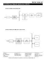
TXCP_50
Transmit
CCPM
PLCP/cell
TRAN
J2, E3 OR DS3
Line
FRMR
J2, E3 or DS3
Line
XBOC
Receive
TDFR
Receive
Transmit
1/2 TTB
Transmit
SPLT
Transmit
ATM and
PLCP
Framer
ATMF/SPLR
Receive
ATM and
PLCP
Framer
TXFF
Transmit
RXCP_50
Receive
RXFF
Receive
4-Cell
MPIF
Microprocessor
System
RCLK
RPOS/RDAT
RNEG/RLCV/ROHM
TCLK
TPOS/TDATO
TNEG/TOHM
1/2 TTB
Receive
PMON
Perfor-
mance
RFDL
Receive
RBOC
Receive
Receive
O/H
RO
H
RO
H
C
LK
RO
H
F
P
TO
HI
NS
TO
H
TO
HC
LK
TO
H
F
P
R
C
ELL
A[
10:
0
]
ALE
CS
B
WRB
RD
B
IN
TB
D
[7:
0]
RS
T
B
SI
G R
1
SI
G
R
5
SI
G R
4
SI
G R
3
SI
G R
2
PR
GD
BER
IEEE
P1149.1
TDO
TC
K
TDI
TMS
TRS
T
B
S
IG
T
1
SI
G T
2
SI
G
T
3
SI
G
T
4
SI
G T
5
S
IG
T
7
S
IG
T
6
DTCA
TDAT [15:0]
TPRTY
TSOC
TCA
TADR [2:0]
TENB
TFCLK
PHY_ADR[2:0]
ATM8
RFCLK
RENB
RADR [2:0]
RCA
RSOC
RPRTY
RDAT [15:0]
DRCA
SIG T1: TPOHINS
SIG T2: TPOH/TDAT
SIG T3: TIOHM/TFP/TMFP
SIG T4: TICLK
SIG T5: TPOHCLK
SIG T6: TPOHFP/TFPO/TMFPO/TGAPCLK/TCELL
SIG T7: REF8KI
SIG R1: FRMSTAT
SIG R2: RPOCHCLK/
RSCLK/RGAPCLK
SIG R3: REF8KO/
RPOHFP/RFPO/RMFPO
SIG R4: RPOH/ROVRHD
SIG R5: LCD/RDATO
BLOCK DIAGRAM


