background image


PEX 8680 Quick Start Hardware Design Guide, Version 1.1 

12 

© 2011 PLX Technology, Inc. All Rights Reserved. 

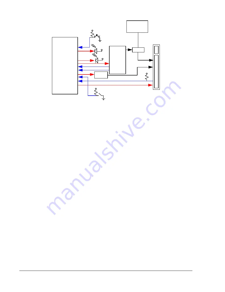
Clkenx#

Atnledx#

Pwrledx#

Pwrenx

Perstx#

VCC

System 

Power 

Supply

12V, 3.3V

VCC

VCC

Buttonx#

Pwrflx#

Mrlx#

Prsntx#

VCC

VCC

Hot Plug 

Controller

Pwrgdx#

Clken_a#

Atnled_a#

Pwrled_a#

Pwren_a

Perst_a#

Button_a#

Pwrflt_a#

Mrl_a#

Prsnt_a#

Pwrgood_a

PEX 8680

FETs

Clock 

Buffer


Figure 13. PHPC Circuit Block Diagram 

 
When connecting the I

2

C-Port 1 to multiple I/O expander ICs, the PEX 8680 has the option of having Hot 

Plug capability on eight of its downstream Ports. The PEX 8680’s I

2

C-Port 1 is the I

2

C Master, which is 

designed to interface to I/O expander ICs, to build SHPCs. One 16-I/O expander connects to I

2

C-Port 1 

for a single SHPC, and one 40 I/O expander connects to the I

2

C-Port 1 for two SHPCs. Both 16-I/O 

expander(s) and 40-I/O expander(s) cannot concurrently connect to the I

2

C Bus. To use 40-I/O 

expander(s), a register bit within the PEX 8680 must be Set, and boot with serial EEPROM is essential. 
After the PEX 8680  is powered up, the state machine inside the PEX 8680  scans the number of I/O 
expander ICs connecting to the I

2

Figure  14

C Bus, starting from Address 000h, in ascending order. If it cannot 

locate the device with Address 000h, it stops the scan process. After it locates the I/O expander IC, it 
automatically assigns a valid Port Number for this SHPC. 

  illustrates a block diagram of the 

SHPC interface to the PEX 8680. The SHPC has more signals than the PHPC. Besides the 10 Hot Plug 
signals mentioned at PHPC, INTERLOCK, SLOTID[3:0], and one GPIO are added to the SHPC. Also, the 
interrupt signal output, INT#, from the I/O expander, should be connected to the PEX 8680’s Interrupt 
Input ball, SHPC_INT#, for the PEX 8680  to service input events at the SHPC.  Because the I/O 
Expander requires some time to be configured upon power-up, it is recommended that GPIO[24-42] 
signals  from the PEX 8680  be  used for slot  PERST# from the I/O Expander to provide reset to 
downstream slots. 

Содержание PEX 8680

Страница 1: ...0 Quick Start Hardware Design Guide Version 1 1 August 2011 Website www plxtech com Technical Support www plxtech com support Copyright 2011 by PLX Technology Inc All Rights Reserved Version 1 1 Augus...

Страница 2: ...e without notice Products may have minor variations to this publication known as errata PLX assumes no liability whatsoever including infringement of any patent or copyright for sale and use of PLX pr...

Страница 3: ...ation relating to the quality content or adequacy of this information The information in this document is subject to change without notice Although every effort has been made to ensure the accuracy of...

Страница 4: ...BGA Routing Escape and De Coupling Capacitor Placement 6 2 2 Add in Board Routing 8 2 3 System Board Routing 8 2 4 Midbus Routing 9 2 5 PCB Stackup Considerations 9 3 Non Transparent Function 10 4 I2...

Страница 5: ...In Card Routing to PCI Express Gold Fingers 8 Figure 8 System Board Routing to PCI Express Slot 8 Figure 9 PCI Express Midbus Routing Example 9 Figure 10 Enable NT Function with NT Strapping Balls 10...

Страница 6: ...PEX 8680 Quick Start Hardware Design Guide Version 1 1 vi 2011 PLX Technology Inc All Rights Reserved THIS PAGE INTENTIONALLY LEFT BLANK...

Страница 7: ...xpress Base Specification Revision 2 0 continues to mature so does its description of the Physical Layer Electrical sub block A PCI Express serial Link is described in terms of four components Transmi...

Страница 8: ...e role of de emphasis is to reduce the amount of energy used to transmit multiple successive bits of the same polarity that is non transition bits compared to the amount of energy used to transmit a s...

Страница 9: ...ster levels are added together for non transition bits the two values are subtracted Using Equation 1 Example 1 presents a calculation of what the drive level and de emphasis level would be for a give...

Страница 10: ...has a 4 bit control word Table 1 describes the Receiver equalization effects Table 1 Receiver Equalization Settings SerDes N Receiver Equalizer 3 0 Equalization 0000b Off 0010b Low 0110b Medium 1110b...

Страница 11: ...Clock source This delay should not exceed 12 ns per PCI Express specification The delay budget includes on chip and off chip delays In general terms all Reference Clock nets in a system should be matc...

Страница 12: ...tromechanical CEM Specification defines two platforms referred to as system boards and add in cards boards Each platform has its own criteria in terms of jitter and loss budget trace lengths and lengt...

Страница 13: ...k Start Hardware Design Guide Version 1 1 2011 PLX Technology Inc All Rights Reserved 7 Figure 5 Top Layer BGA Layout and Routing Escape Figure 6 Bottom Layer BGA Layout Escape and De coupling Capacit...

Страница 14: ...and into the inner rows of the BGA The layer transition should occur at the midbus footprint if one exists or close to the gold fingers Either location should have plenty of ground vias PCI Express ad...

Страница 15: ...s is enough to determine the characteristic impedance of that trace For differential signals the last step is to determine the separation between the positive and negative conductors to achieve the ne...

Страница 16: ...Port Method 2 Enable the NT function and configure the NT Port through the serial EEPROM The NT configuration settings will be loaded upon power up and after reset Method 3 Use the PEX 8680 I2 C Port...

Страница 17: ...to the PEX 8680 is illustrated in VCC PEX 8680 I2C_SDA0 I2C_SCL0 VCC 1 2 R R R 1K to 10K Figure 12 I 2 C Interface Block Diagram 5 Hot Plug Circuitry The PEX 8680 supports four Parallel Hot Plug Cont...

Страница 18: ...40 I O expander s a register bit within the PEX 8680 must be Set and boot with serial EEPROM is essential After the PEX 8680 is powered up the state machine inside the PEX 8680 scans the number of I...

Страница 19: ...O 10 7 26 22 IO 11 27 IO 12 28 IO 15 31 VCC VCC GPIO VCC Figure 14 SHPC Interface to PEX 8680 Block Diagram 6 JTAG Interface The PEX 8680 supports a five ball JTAG Boundary Scan interface The JTAG int...

Страница 20: ...he optional Debug function is primarily intended for prototyping activities Its use requires assistance from PLX Technical Support Two major debug functions of the PEX 8680 are External Probe mode EPM...

Страница 21: ...t_sel1 ln2_add2 HP_MRL_D port_sel0 ln2_add1 HP_MRL_A outA_sel3 HP_BUTTON_A outA_sel2 HP_PWR_GOOD_C outA_sel1 ln_sel1 HP_PRSNT_C outA_sel0 ln_sel0 HP_BUTTON_D outB_sel3 ln2_add0 HP_PWR_GOOD_A outB_sel2...

Страница 22: ...A11 xmit_dat11 HP_CLKEN_C prb_outA10 xmit_dat10 HP_PWRLED_C prb_outA9 xmit_dat9 HP_ATNLED_D prb_outA8 xmit_dat8 HP_CLKEN_A prb_outA7 xmit_dat7 HP_PWREN_C prb_outA6 xmit_dat6 HP_ATNLED_C prb_outA5 xmit...

Страница 23: ...the Gen 2 data rate and Autonomous Change When this ball is tied Low if the Link training sequence fails during configuration the next time the LTSSM exits the detect state TS Ordered Sets advertise o...

Страница 24: ...OD 23 0 and GPIO 42 24 signal functionality NOTE 00h is not a valid setting For normal operation these balls should be pulled to 0Dh by external pull ups Internal pull downs STRAP_UPSTRM_PORTSEL 4 0 U...

Страница 25: ...variance on the supply rails due to noise and IR drop VDD25 power is used for the single ended I O buffers Hot Plug serial EEPROM JTAG I 2 11 2 Power Sequencing C and the Port Status indicators Althou...

Страница 26: ...ately 200 pF in2 As for discrete capacitors the footprint and physical size of discrete capacitors have a significant effect on the frequencies in which the capacitors provide effective de coupling To...

Страница 27: ...lower frequency components The proximity of these capacitors is not critical therefore they can be placed outside the BGA matrix It is strongly recommended to measure the attenuation versus frequency...

Страница 28: ...Data Book Version 1 0 or higher PCI Special Interest Group PCI SIG 3855 SW 153rd Drive Beaverton OR 97006 USA Tel 503 619 0569 Fax 503 644 6708 www pcisig com PCI Local Bus Specification Revision 3 0...

Отзывы: