PEX 8680 Quick Start Hardware Design Guide, Version 1.1
© 2011 PLX Technology, Inc. All Rights Reserved.
9
2.4
Midbus Routing
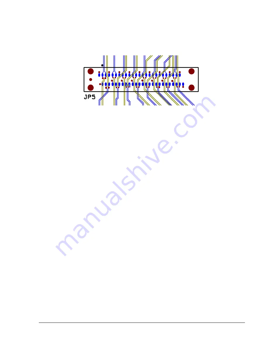
Midbus footprints can be placed into the routing path, to provide an interface to various protocol analyzers,
as well as provide a location to probe a signal using oscilloscopes. Transmitter pairs route on one side of
the footprint, while Receiver signals route through the other side.
Figure 9. PCI Express Midbus Routing Example
2.5
PCB Stackup Considerations
Determining the PCB stackup is one of the most important steps in designing and implementing a system.
The PCB stackup should be determined prior to board routing, because it will determine the trace width
and spacing requirements necessary to achieve a particular characteristic impedance and differential
impedance. After the stackup is known, the trace width can be selected. For a single-ended signal, this is
enough to determine the characteristic impedance of that trace. For differential signals, the last step is to
determine the separation between the positive and negative conductors, to achieve the needed
differential impedance.
Additionally, a PCB stackup can determine the power supply de-coupling scheme for a device. Parallel
plane capacitance exists between a PCB’s DC power and ground planes. PCB reference planes have an
insignificant amount of series inductance; therefore, their effective frequency range is much higher than
that of discrete capacitors.
PCB traces can be implemented as one of two types of transmission lines – microstrip and stripline.
Microstrip traces have only one reference plane, and therefore, represent traces on the outer layers (top
and bottom layer) of a PCB. Stripline traces have two reference planes and are implemented using inner
routing layers. Typically, stripline traces are only available for PCBs with six or more layers. Microstrip
and stripline traces each have their own properties, which must be weighed when determining which type
of trace to use.


