PDP-425CMX
70
1
2
3
4
1
2
3
4
C
D
F
A
B
E
6.2 ADJUSTMENT
Adjusting conditions
Adjustments should be carried out in the procedures below. However, any adjustments other than the below are not
required.
•
•
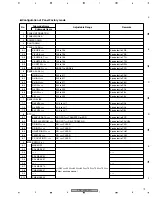
When the "PDP module" is replaced, adjustmentsshould conform to the adjusting items below.
[HOW TO CLEAR HISTORY DATA] [BACKUP WHEN THE MAIN UNIT IS ADJUSTED]
When the "MAIN Assy" is replaced, adjustments should conform to the adjusting item of
[ 1, 2 ] specified below.
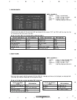
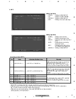
MONITOR INFORMATION
MODEL NAME
: PDP-425CMX
SERIAL/NUMBER
:
SOFT WARE VERSION
: C123
USAGE TIME
: 00000H
T1 025
T2 025
T3 025
T4 - -
[MENU/ENTER] NEXT [EXIT] PREV 9/10
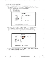
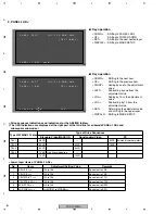
MONITOR INFORMATION
MODEL NAME
: PDP-425CMX
SERIAL/NUMBER
SOFT WARE VERSION
: C123
USAGE TIME
: 00000H
T1 025
T2 025
T3 025
T4 - -
[MENU/ENTER] NEXT [EXIT] PREV 9/10
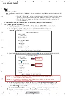
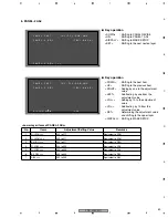
1. Adjustments after the replacement of the MAIN Assy (Using the remote control)
1-1. Product serial No. registration
Press the keys in the order of [
PIP SHIFT
]
→
[
SET
]
→
[
Clear
]
→
[
PIP SHIFT
] in order to enter the
factory adjustment menu.
Press the [
Clear
] or [
ID No. set
] key to select the [MONITOR INFORMATION] No. menu.
(Example : PDP-425CMX)
Press the [
SCREEN SIDE
] key 4 times to display a cursor in the lower column of [SERIAL/NUMBER].
(Caution 1) No modification is possible here because this modification is already finished by 3-2.
Factory shipment setting (initial setting).
(Caution 2)
No modification is possible here because registration is already finished at the time of
shipment in terms of maintenance parts.
(Caution 1)
(Caution 2)
(1)
(2)
(3)
2
3
5
∞
Moving the POSITION/CONTROL keys of [ ] and [ ], select the numerals and characters of the
serial number that is listed in the serial label located on the rear surface of the product. Register the
serial number. (Blank
→
0 to 9
→
A to Z)
Moving the POSITION/CONTROL keys of [ ] and [ ], select the next digit by means of a cursor.
(6)
(5)
(4)
Repeat the processes of (4) and (5) above and register the serial number completely.
Содержание PDP-42MXE10
Страница 9: ...PDP 425CMX 9 5 6 7 8 5 6 7 8 C D F A B E ...
Страница 26: ...PDP 425CMX 26 1 2 3 4 1 2 3 4 C D F A B E 3 2 OVERALL CONNECTION DIAGRAM 2 2 Overall Wiring Diagram 2 2 ...
Страница 27: ...PDP 425CMX 27 5 6 7 8 5 6 7 8 C D F A B E ...
Страница 37: ...PDP 425CMX 37 5 6 7 8 5 6 7 8 C D F A B E ...
Страница 129: ...PDP 425CMX 129 5 6 7 8 5 6 7 8 C D F A B E ...
Страница 132: ...PDP 425CMX 132 1 2 3 4 1 2 3 4 C D F A B E MAIN PWB CONNECTOR WAVE FORM POINT SIDE B ...
Страница 133: ...PDP 425CMX 133 5 6 7 8 5 6 7 8 C D F A B E X5008 X5008 34 35 IC6304 IC6302 29 29 IC6302 29 SIDE B ...
Страница 178: ...PDP 425CMX 178 1 2 3 4 1 2 3 4 C D F A B E Pin Layout Block Diagram DS90CF388VJD MD DIGITAL ASSY IC3001 LVDS Receiver ...

