2-1
2-1
DISMANTLING INSTRUCTIONS
Dismantling of the Front Panel assembly
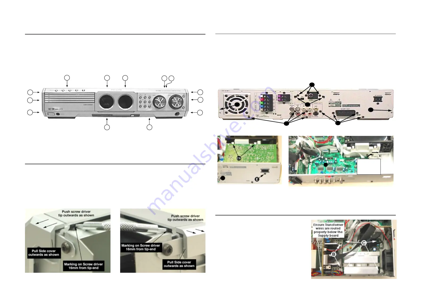
1) Loosen the 9 screws to dismantle the Top Cover (pos
252)
- 2 screws on each side
- 5 screws on the Rear Panel (pos 251).
Dismantling the Tuner, Mains and AV boards
2) Loosen 5 screws A and 8 catches C1 to slide the Front
Panel assembly (pos 101, 102, 103, etc) as per figure 1.
Note: To remove the Source / Volume control pc
board (pos 1105B) 2 nuts hidden below the
control knob assembly (pos 133, 134 and 135)
must first be removed.
Hints for re-assembly of Top Cover
Due to appearance design the Top cover (pos 252) is
sandwiched between the Front panel (pos 101) and the 2
side covers (pos 102 & 103), this make it necessary to
remove the 2 side covers before re-assembly of Top cover.
1) To remove the side cover use a small screw driver with
marking 16mm from the tip end.
2) Insert the screw driver into slot (as shown in figure 2) and
push the tip outwards to release the side cover catch.
The side cover can be pull outwards as soon as the top
catch is released.
Figure 2
1) Loosen 3 screws D and 2 catches C2 on the Rear panel
(pos 251) to remove the Tuner board assemby (pos 1101)
as pe figure 3.
2) Loosen 1 screws E and 2 catches C3 to unslot the Mains
board (pos 1102-A) out of the Rear panel as per figure 4.
3) Loosen bracket (pos 254) by turning a catch, sliding
towards the outside and lifting it upwards as per figure 5.
4) Loosen 8 screws F (7 screws for non-Scart version) and
2 catches C5 to separate Rear Plate assembly (pos 251)
from the Bottom plate assembly (pos 227) as per figure
3.
5) Uncatch C4 to remove the AV board (pos 1104) from the
Bottom Plate assembly (pos 227) as per figure 5.
Figure 3
C5
D
F
F
C5
C2
A
A
A
A
C1
C1
C1
C1
C1
C1
A
C1
C1
Figure 1
Figure 5
C4
1
2
Turn up the lever,
slide the bracket
as shown and lift
out of the bottom
chassis.
Figure 4
Dismantling the Supply & Power Amplifier boards
1) Loosen 2 screws B mounting the Supply board's (pos
1102-B) heatsink to the Bottom Plate (pos 227) as per
figure 6.
Note: During re-assembly care must be taken to
ensure the Mains Transformer wires to the
Supply board is routed properly below the
board.
2) Loosen 4 screws C to dismantle the Power Amplifier
board (pos 1102-D) from the Bottom Plate as per figure
6.
Figure 6
Содержание MX5800SA
Страница 60: ...8239 210 93436 3139 113 3494pt6 dd wk0334 PART B 8 9 8 9 MAINS ECO STBY BOARD CHIP LAYOUT PART B ...
Страница 62: ...8 9a 8 9a MAINS ECO STBY BOARD CHIP LAYOUT PART B For pcb layout 34948 3139 113 3494 pt8 dd wk0350 PART B ...
Страница 68: ...8239 210 93416 3139 113 3494pt6 dd wk0334 PART B 8 13 8 13 SUPPLY BOARD CHIP LAYOUT PART B ...
Страница 70: ...8 13a SUPPLY BOARD CHIP LAYOUT PART B For pcb layout 34948 3139 113 3494 pt8 dd wk0350 PART B 8 13a ...
Страница 76: ...3104 213 3525p5 dd wk0334 PART B 8 19 8 19 AMPLIFIER BOARD BOTTOM VIEW PART B ...
Страница 78: ...3104 213 3525p5 dd wk0334 PART D 8 21 8 21 AMPLIFIER BOARD TOP VIEW PART D ...
Страница 91: ...9 10 9 10 BOTTOM VIEW PART C PART C ...
Страница 92: ...9 11 9 11 BOTTOM VIEW PART D PART D 3139 113 3500 pt6 dd wk334 ...
Страница 95: ...9 14 9 14 BOTTOM VIEW PART G PART G ...
Страница 96: ...9 15 9 15 BOTTOM VIEW PART H PART H 3139 113 3500 pt6 dd wk334 ...
Страница 104: ...10 5 10 5 Exploded view 5DTC mechanic for orientation only ...
Страница 111: ...BOTTOM VIEW COMPONENT LAYOUT For pcb layout 35037 11 4a 11 4a 3139 113 3503 pt 7 dd wk414 ...
Страница 112: ...TOP VIEW PART A 11 5 11 5 PART A ...
Страница 113: ...TOP VIEW PART B 11 6 11 6 PART B ...
Страница 115: ...TOP VIEW PART B For pcb layout 35037 11 6a 11 6a 3139 113 3503 pt 7 dd wk414 PART B ...
Страница 126: ...12 1 12 1 EXPLODED VIEW MAIN UNIT MX5800SA exploded view 3139 119 35170 dd wk318 ...


