3-1
3-1
Various
other Tests
Activated with
ACTION
TEST
S
EEPROM FORMAT
TEST
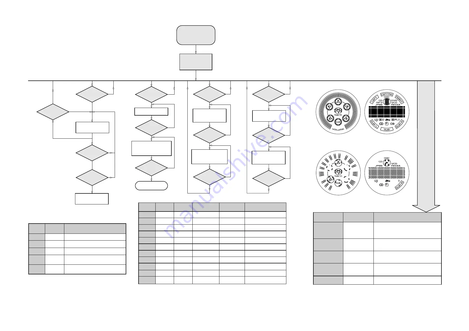
Load default data. Display shows "NEW" for 1 second.
Caution!
All presets from the customer will be lost!!
Disconnect
mains cord
LEAVE SERVICE
TEST PROGRAM
T
9
to Exit
EEPROM TEST
Some test patterns will be sent to the EEPROM.
"PASS" is displayed if the uProcessor read back
the test patterns correctly, otherwise "FAIL" will be
displayed.
SUBW +
(Remote Control)
AUTO STANDBY
TOGGLE
Pressing this button will toggle between the status
"AUTO STANDBY ON" and "AUTO STANDBY OFF".
The status will scroll once across the Display.
SOURCE / VOLUME
Knob
ROTARY
ENCODER TEST
Display shows value for 2 seconds.
Values increases or decreases in steps of 1 until
0 (Min.) or 40 (Max.) is reached.
Figure 2
Figure 1
Y
N
Y
N
N
B
II
Button pressed?
B
II
Button pressed?
DISPLAY
TEST
Display shows Figure 1
and Standby LED is
Green
Display shows Figure 2
and Standby LED is
RED
Y
9
Button pressed?
Y
N
Y
N
SEATING
Button pressed?
ADC
TEST
Display shows
"ADC Value"
(Ref Table 1)
Y
N
9
Button pressed?
Note:
ADC Test is used for checking the ADC inputs to the microprocessor. The display
shows an ADC value between 0 and 255 for an input signal between 0 and 5V.
N
SEATING
Button pressed?
Y
Display shows next
"ADC Value"
(Refer Table 1)
Has it reach
"ADC5 Value" ?
Table 1
Name
ADC1
ADC2
ADC3
ADC4
ADC5
Input line to
uProcessor IC
Key0
Key1
VU_IN
MUX_DET
Options
Remarks
Return the value assign for each key button.
Return the value assign for each key button.
Varies according to the signal dc level
The set temperature is measured via this NTC
line, if lower than 69 the set goes into Standby.
Return the value assign for the different possible
options
CLOCK-TIMER
Button pressed?
Y
Y
Y
N
N
N
CLOCK-TIMER
Button pressed?
9
Button pressed?
Display shows
32K
Output at (Front Board)
pin 19 of uP = 2048Hz
Display shows
12M
Output at (Front Board)
pin 19 of uP = 2,929.6875Hz
QUARTZ
TEST
TUNING
Button pressed?
Disconnect
Mains cord ?
Y
Y
N
N
Y
Display Tuner Version
"ccc"
Service frequencies are
copied to the RAM (see Table 2)
Tuner works normally except:
PROGRAM button
Service Mode left
TUNER
TEST
TUNING
Button pressed?
N
PRESET
1
2
3
4
5
6
7
8
9
10
11
Europe
"EUR"
87.5MHz
108MHz
531kHz
1602kHz
558kHz
1494kHz
87.5MHz
87.5MHz
87.5MHz
87.5MHz
98MHz
USA
"USA"
87.5MHz
108MHz
530kHz
1700kHz
560kHz
1500kHz
98MHz
87.5MHz
87.5MHz
87.5MHz
87.5MHz
Oversea
"OSE"
87.5MHz
108MHz
530/531kHz*
1700/1602kHz*
560/558kHz*
1500/1494kHz*
98/87.5MHz*
87.5MHz
87.5MHz
87.5MHz
87.5/98MHz*
Note: * Depending on the selected grid frequency (9 or 10kHz).
By holding the "DISC5" and "STANDBY-ON" buttons depressed while switching on the Mains supply, one of the
undermentioned features will be activated:
- the tuning grid frequency is toggled between 9kHz and 10kHz for the Oversea (/21) version.
Table 2
East Europe
"EAS"
87.5MHz
108MHz
531kHz
1602kHz
558kHz
1494kHz
87.5MHz
87.5MHz
87.5MHz
87.5MHz
98MHz
East Eur. Extended-band
"EAS"
65.81MHz
108MHz
74MHz
87.5MHz
531kHz
1602kHz
558kHz
1494kHz
98MHz
70.01MHz
65.81MHz
To start service test program
hold DISC1 & STANDBY-ON
buttons depressed while
plugging in the mains cord*
Display shows the
ROM version
"S-Vyy"
S refers to Service Mode
V refers to Version
yy refers to Software version number of the uProcessor
(counting up from 01 to 99)
SERVICE TEST PROGRAM I
5DTC MX.. Range Service Test Program dd wk0302
MAIN MENU
* Hold till the Display is shown
Содержание MX5800SA
Страница 60: ...8239 210 93436 3139 113 3494pt6 dd wk0334 PART B 8 9 8 9 MAINS ECO STBY BOARD CHIP LAYOUT PART B ...
Страница 62: ...8 9a 8 9a MAINS ECO STBY BOARD CHIP LAYOUT PART B For pcb layout 34948 3139 113 3494 pt8 dd wk0350 PART B ...
Страница 68: ...8239 210 93416 3139 113 3494pt6 dd wk0334 PART B 8 13 8 13 SUPPLY BOARD CHIP LAYOUT PART B ...
Страница 70: ...8 13a SUPPLY BOARD CHIP LAYOUT PART B For pcb layout 34948 3139 113 3494 pt8 dd wk0350 PART B 8 13a ...
Страница 76: ...3104 213 3525p5 dd wk0334 PART B 8 19 8 19 AMPLIFIER BOARD BOTTOM VIEW PART B ...
Страница 78: ...3104 213 3525p5 dd wk0334 PART D 8 21 8 21 AMPLIFIER BOARD TOP VIEW PART D ...
Страница 91: ...9 10 9 10 BOTTOM VIEW PART C PART C ...
Страница 92: ...9 11 9 11 BOTTOM VIEW PART D PART D 3139 113 3500 pt6 dd wk334 ...
Страница 95: ...9 14 9 14 BOTTOM VIEW PART G PART G ...
Страница 96: ...9 15 9 15 BOTTOM VIEW PART H PART H 3139 113 3500 pt6 dd wk334 ...
Страница 104: ...10 5 10 5 Exploded view 5DTC mechanic for orientation only ...
Страница 111: ...BOTTOM VIEW COMPONENT LAYOUT For pcb layout 35037 11 4a 11 4a 3139 113 3503 pt 7 dd wk414 ...
Страница 112: ...TOP VIEW PART A 11 5 11 5 PART A ...
Страница 113: ...TOP VIEW PART B 11 6 11 6 PART B ...
Страница 115: ...TOP VIEW PART B For pcb layout 35037 11 6a 11 6a 3139 113 3503 pt 7 dd wk414 PART B ...
Страница 126: ...12 1 12 1 EXPLODED VIEW MAIN UNIT MX5800SA exploded view 3139 119 35170 dd wk318 ...


