


1 - 1
HTS5200
/12/98/51
©
Copyright 2010 Philips Consumer Electronics B.V. Eindhoven, The Netherlands
All rights reserved. No part of this publication may be reproduced, stored in a retrieval system or
transmitted, in any form or by any means, electronic, mechanical, photocopying, or otherwise
without the prior permission of Philips.
Published by
RY1014
Service Audio Printed in The Netherlands Subject to modification
DVD Home Theater System
Version 1.1
TABLE OF CONTENTS
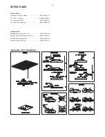
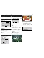
Location of PCB Boards ............................................ 1-2
Versions Variation ...................................................... 1-2
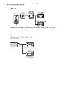
Measurement Setup .................................................. 1-4
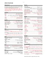
Specifications ............................................................ 1-3
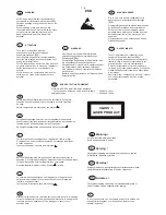
Service Aids .............................................................. 1-5
ESD & Safety Instruction .......................................... 1-6
Lead-free soldering Information ................................ 1-7
Setting procedure & Repair Instructions........................ 2
Disassembly Instructions & Service positions .............. 3
Block & Wiring Diagram ................................................ 4
VFD+USB+AUX Board .................................................. 5
Main+LED Board............................................................ 6
Power Board .................................................................. 7
Service Manual
Service
Tfswjdf
Service
Tfswjdf
Service
AMP Board .................................................................... 8
Touch Board .................................................................. 9
Mechanical Exploded view .......................................... 10
Revision List ................................................................ 11
GB
Chapter
3139 785 35301
Содержание HTS5200
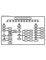
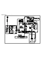
Страница 9: ...2 2 2 2 REPAIR INSTRUCTIONS One ...
Страница 10: ...2 3 2 3 REPAIR INSTRUCTIONS Two ...
Страница 11: ...2 4 2 4 REPAIR INSTRUCTIONS Three ...
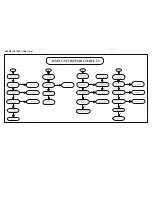
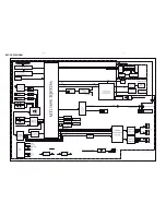
Страница 15: ...4 1 4 1 BLOCK DIAGRAM ...
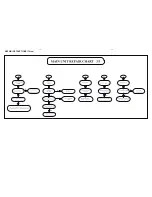
Страница 16: ...4 2 4 2 WIRING DIAGRAM V3 V4 V1 V2 ...
Страница 33: ...9 1 9 1 TOUCH BOARD TABLE OF CONTENTS Circuit Diagram 9 2 PCB Layout Top View Bottom View 9 3 ...
Страница 37: ...11 1 REVISION LIST Version 1 0 Initial release Version 1 1 Update chapter 1 2 ...