Circuit Descriptions, List of Abbreviations, and IC Data Sheets
EN 94
DPTV565 AA
9.
9.5
Control/OSD
9.5.1
Microprocessor
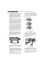
Figure 9-40 Micro processor
The HDR2K3 has two microprocessors. The microprocessor,
OTC, located on the SSB, 7001, is the main processor for the
set. When Power is applied to the set and the Mains switch is
turned "on", the processor monitors the Keyboard and IR
receiver located on the Sensor Board. This IC controls the
functions on the SSB, Video switching on the SSM, and the
PIP/DW panel. A ROM located inside the IC has the Startup
program. The main program to run the processors is located in
the Program Flash RAM, 7006. IC 7012 is used by the OTC for
temporary storage. IC 7007 is used to store data for Teletext.
There are three I2C busses, a fast bus, F, a slow bus, S, and a
TX bus to communicate with the microprocessor on the ACS
module. The NVM 7011 stores settings such as customer
preferences, OPT numbers, Tuner settings, and Error codes.
composite video is fed to pin 5 for decoding Teletext and
Closed Caption information. In the Standby mode, Power is not
applied to the processor on the ACS module.
The microprocessor, 7100, located on the ACS module,
controls the Convergence, Geometry, and CRT drive circuits.
Settings for Convergence, Geometry, and White drive are
stored in the NVM, 7000. This IC is 512K for the AP sets and
256K for the Korean version. When 7100 reads the size of
7000, it then determines which software to load. If it reads 512K
present, the AP software is loaded. If it reads 256K, NTSC only
software is loaded. Commands for the ACS processor are
produced by the OTC on the SSB and transmitted via the TXD
and RXD lines.
9.5.2
Front Control Panel
Figure 9-41 Front Control Panel
The Front Control panel has the Power LED, Keyboard, IR
Receiver, and Light Sensor. The Keyboard is a resistor ladder.
The voltage changes value depending on which selection is
made. The voltage on this line will be 3.3 volts if no buttons are
selected. The two-colour LED indicates the status of the set. In
the Standby mode, the ON_OFF_LED line is High and the +9-
volt source is turned "off". In this case, the RED LED is lit.
When the set is turned "on", the +9-volt source is switched "on",
turning the Green section of the LED "on". The LED then turns
Yellow. When the set is fully "on", the ON_OFF_LED line goes
Low, turning the Red LED "off". The indicator is now Green.
The IR Receiver, 6105, receives commands from the remote
control.
KEYBOARD
1201
ON/OFF
LED
STBY
LED
LIGHT
SENSOR
RC5
5
4
6
7
1014
2
5
4
6
7
1020
79
77
37
78
107
113
104
116
100
74
83
84
5
7010
7015
7016
HFB
VSYNC
CVBS-TXT
RESET
SENSOR
BOARD
SSM
SSB
86
85
88
87
91
92
SDA-S
SCL-S
SDA-F
SCL-F
5
6
7011
NVM
SDA
SCL
7001
OTC
PROGRAM
FLASH
RAM
EPG
FLASH-RAM
DRAM
TXT
7006
7012
7007
DTA
ADD
45-66
23-37
STANDBY
2
+3.3V
ACS
SDA-B
SCL-B
SDA-C
SCL-C
1200
7000
NVM
75
82
81
28
13
84
83
69
70
52
48
47
46
WC
+5V
5
6
7
8
1
BLANK-UP
RED-UP
GRN-UP
BLUE-UP
55
53
SYNC-V
SYNC-H
7100
ACS
CONTROL
16
17
30
RESET
72
CONV
90
89
E_15000_110.eps
181004
+9V
PROC
TO HOP
VIA
SSM
SSM
TxD
RxD
1401-2
1401-4
1043-9
1043-7
1000-1
1000-2
2
3
5
4
1
7
6
1201
6102
6.8V
6103
6.8V
6101
RED
GREEN
3121
560
+9V
1
2
3
3107
330
3108
6.8K
3114
10K
3109
470
RC5
LIGHT_SENSOR
1401
PO
WER
3101
100
1402
VO
L+
1403
3102
240
VO
L-
CH+
CH-
3103
470
1404
MENU
3104
820
ASC
3105
1.5K
1406
3106
3.6K
1407
1405
6105
IR
REC
KEYBOARD
GND
ON_OFF_LED
+9V
+5V_STANDBY
RC5
LIGHT_SENSOR
E_15000_111.eps
181004
Содержание DPTV565 AA
Страница 27: ...Circuit Diagrams and PWB Layouts 27 DPTV565 AA 7 Layout SSB Top Side E_15000_133 eps 191004 8204 000 6507 3 ...
Страница 29: ...Circuit Diagrams and PWB Layouts 29 DPTV565 AA 7 Layout SSB Bottom Side E_15000_134 eps 191004 8204 000 6507 3 ...
Страница 41: ...Circuit Diagrams and PWB Layouts 41 DPTV565 AA 7 Layout SSM Part 1 Bottom Side F_15020_011a eps 110305 Part 1 ...
Страница 42: ...42 DPTV565 AA 7 Circuit Diagrams and PWB Layouts Layout SSM Part 2 Bottom Side Part 2 F_15020_011b eps 110305 ...
Страница 43: ...Circuit Diagrams and PWB Layouts 43 DPTV565 AA 7 Layout SSM Part 3 Bottom Side F_15020_011c eps 110305 Part 3 ...
Страница 44: ...44 DPTV565 AA 7 Circuit Diagrams and PWB Layouts Layout SSM Part 4 Bottom Side F_15020_011d eps 110305 Part 4 ...
Страница 72: ...72 DPTV565 AA 7 Circuit Diagrams and PWB Layouts Personal Notes E_06532_013 eps 131004 ...
Страница 119: ...Revision List EN 119 DPTV565 AA 11 11 Revision List Manual xxxx xxx xxxx 0 First release ...

