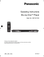
manualshive.com logo in svg
background image

BDP3200(X)

/51/55/77/78

©

 Copyright 2011 Philips Consumer Electronics B.V. Eindhoven, The Netherlands

All rights reserved.  No part of this publication may be reproduced, stored in a retrieval system or 
transmitted, in any form or by any means, electronic, mechanical, photocopying, or otherwise without 
the prior permission of Philips.
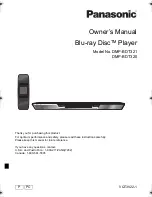
Blu-ray Disc Player

Version 1.1

Version 0.0

LASER PRODUCT

CLASS 1

314178535911

Published by CY_SL1108  BG AVM   Printed in The Netherlands    Subject to modification

TABLE OF CONTENTS


        Chapter 


Technical Specification, PCBs Location…………………..  1 
Safety Instruction ……………………………………………… 2 
Instruction for Use……………………………………………… 3 
Mechanical and Dismantling Instructions…………………. 4 
Service Modes, Troubleshooting……………………………. 5 
Overall Block Diagram, Wiring Diagram……………………. 6 
Electrical Diagram……………………………………………… 7 
Exploded View Diagram & Service Part List………………..8 
Revision List…………………………………………………….  9 


Содержание BDP3200/51

Страница 1: ...the prior permission of Philips Blu ray Disc Player Version 1 1Version 0 0 LASER PRODUCT CLASS 1 314178535911 Published by CY_SL1108 BG AVM Printed in The Netherlands Subject to modification TABLE OF CONTENTS Chapter Technical Specification PCBs Location 1 Safety Instruction 2 Instruction for Use 3 Mechanical and Dismantling Instructions 4 Service Modes Troubleshooting 5 Overall Block Diagram Wiri...

Страница 2: ...ate MP3 112 kbps 320 kpbs WMA 48 kpbs 192 kpbs USB Compatibility Hi Speed USB 2 0 Class support UMS USB Mass Storage Class Power supply rating AC 220 240V 50 Hz Power consumption 25 W Power consumption in standby mode 0 5 W Dimensions w x h x d 435 x 60 x 227 mm Net Weight 2 35 kg Accessories supplied Remote control and batteries Audio Video cables Power cable Quick start guide User manual CD ROM ...

Страница 3: ... Versions Service policy Board in used BDP3200 TIPS C Component Lever Repair M Module Lever Repair X OCX 1 2 C 51 55 C M MAIN PCBA VFD DISPLAY PCBA VFD DISPLAY PCBA 30W 2P OPEN PCBA 30 W 2P OPEN PCBA M C C MAIN BOARD 55 C M C M 78 C C 77 C C M ...

Страница 4: ...e the Main board will be Cancel Start damaged entirely 4 Press Right cursor button to choose Start then press OK 5 The software will updagrde and screen will display as below Upgrade is ongoing Please wait Please do not unplug or switch off the device 6 Restart the set B Update software via USB Flash Drive 1 Go to www philips com support to check if the latest software version is available for thi...

Страница 5: ...ord and connect a wire between The two pins of the mains plug 2 Set the mains switch the on position keep the Mains cord unplug 3 Measure the resistance value between the mains plug and the front panel controls and chassis bottom 4 Repair or correct unit when the resistance measurement is less than 1M Ω 5 Verify this before you return the unit to the customer user ref UL standard no 1492 6 Switch ...

Страница 6: ...3 0 Instruction for Use You can download this information from the following websites http www philips com support http www p4c philips com 3 1 ...

Страница 7: ...CTIONS The following guidelines show how to dismantle the player Step1 Remove 6 screws around the Top Cover and then remove the Top Cover Figure1 4 1 Step2 Remove the 8 screws on board to dismantle the DVD BOARD POWER BOARD LED BOARD DECK ...

Страница 8: ...n Replace VU1 or VFD Yes Go Yes No Check 5V 12V 24V voltage on the power and front board SG GR on the front board 1 Check whether bad solder exists on VU1 and pins of VFD 2 Check whether the circuit connected to K1 K2 K3 K4 is broken Fix the connection J3 on front board and CN4 on power board Trouble shooting chart 5 1 Check the signals of the VU1 s Check the VU1 power supply VU1 38 5V and VU1 27 ...

Страница 9: ...gnal is right from the U1 s pin 8 9 Correct connection Yes Go No audio output No Trouble shooting chart 5 2 exists on pins of J7 Check whether bad solder Replace the J7 No Yes Check the U1 power supply U1 1 3 3V and U1 11 5V Yes Replace the U1 ...

Страница 10: ...r remote controller Check whether the remote controller s battery is exhausted or not Check the Power supply board part Replace IR1 NO Trouble shooting chart 5 3 Check the IR1 power supply is OK Check the connection J2 on front board and J502 on main board is broken Yes Fix the connection NO Yes ...

Страница 11: ...Board Can t read disc or can t open the disk door Check 40pin and 8pin cable from main board connection to the loader is normal Check the U900 U902 and the peripheral components near them on the main board NO GO Check whether the DVD loader running is normal Fix the connection NO Yes Trouble shooting chart 5 4 ...

Страница 12: ...the voltage 5V_STB on the front board is normal Check DC5V to AC2 5V switch circuit Refer to No display on VFD Yes 24V 12V and D1 is normal No Check the power board or replace D1 Trouble shooting chart 5 5 Check whether the voltage between VFD s F1 and F2 Check whether the voltage on the front board Yes and buttons do not work ...

Страница 13: ...Load_A HA800 45Pin 0 5mm FFC Connect GND USB USB USBVCC OPEN CLOSE POWER STBY IR STB CLK DATA GND GND VCC VCC GND 12V_P GND 5V_STBY Power_ON 12V_M J2 3_3V RXD TXD GND USB400 J502 Load Load TrayOut HA901 TrayIn 128MB DDR3 SDRAM 64Mx16DDR3 R OUT GND UTXD URXD 3_3V CON801 J506 GND VCC VCC GND 12V_P GND 5V_STBY Power_ON 12V_M VFD POWER STBY OPEN CLOSE KEY STOP PLAY PAUSE KEY IR IR STB CLK DATA GND POW...

Страница 14: ... 3 9K 0603 R110 3 9K 0603 R3 51K 0603 R3 51K 0603 R19 470R 0603 R19 470R 0603 R7 4 7K 0603 R7 4 7K 0603 CB3 100pF 0603 CB3 100pF 0603 J3 5PIN 2 0mmDIP J3 5PIN 2 0mmDIP 1 1 2 2 3 3 4 4 5 5 R26 10K 0603 R26 10K 0603 CB7 0 1uF 0603 CB7 0 1uF 0603 CB13 100pF 0603 CB13 100pF 0603 CB8 100pF 0603 CB8 100pF 0603 R5 22K 0603 R5 22K 0603 CB14 1200PF 0603 CB14 1200PF 0603 CB12 0 1UF 0603 CB12 0 1UF 0603 R20 ...

Страница 15: ... L_0805 R5 15K 1 R5 15K 1 R20 10K R20 10K R928 560 R928 560 R1 NC R1 NC R52 10K R52 10K L1 2 2uH 3A L1 2 2uH 3A FB7 FB100R 2A ASD L_0805 FB7 FB100R 2A ASD L_0805 CE10 220uF 6 3v CE10 220uF 6 3v CE9 220uF 6 3v CE9 220uF 6 3v U5 uP7716AMA5 33 SOT 25 SMD U5 uP7716AMA5 33 SOT 25 SMD VIN 1 GND 2 EN 3 NC 4 VOUT 5 FB714 FB100R 2A ASD L_0805 FB714 FB100R 2A ASD L_0805 C3 2 2uF 10V C3 2 2uF 10V C8 10uF 6 3...

Страница 16: ...3 DVCC18_IO_1 T18 DVCC18_IO_1 V12 DVCC18_IO_1 V16 AVDD12_MEMPLL Y21 AVSS12_MEMPLL W21 TP_MEMPLL AB25 TN_MEMPLL AB24 DGND D22 DGND E21 DGND J10 DGND F21 DGND J16 DGND K11 DGND K13 DGND K15 DGND K17 DGND L10 DGND L11 DGND L12 DGND L13 DGND L14 DGND L15 DGND L16 DGND M11 DGND M12 DGND M13 DGND M14 DGND M15 DGND M17 DGND AA7 DGND M9 DGND N10 DGND N11 DGND N12 DGND N13 DGND N14 DGND N15 DGND N16 DGND N...

Страница 17: ...M9 VSS_8 P1 VSS_9 P9 VSS_10 T1 VSS_11 T9 VDD_6 N9 VDD_7 R1 VDD_8 R9 C234 0 1uF 10V C234 0 1uF 10V C211 0 1uF 10V C211 0 1uF 10V C230 0 1uF 10V C230 0 1uF 10V C222 0 1uF 10V C222 0 1uF 10V C239 0 1uF 10V C239 0 1uF 10V C241 0 1uF 10V C241 0 1uF 10V C220 0 1uF 10V C220 0 1uF 10V R201 240 R201 240 U100B MT8550 U100B MT8550 DVCC10_K J15 DVCC10_K J17 DVCC10_K J9 DVCC10_K K10 DVCC10_K K14 DVCC10_K K16 D...

Страница 18: ..._TPD4S010B TVS Arrays D301 PESD_TPD4S010B 1 1 2 2 GND 3 4 4 5 5 6 6 7 7 GND 8 9 9 10 10 TP304 TP304 TP301 TP301 C307 NC ASD C_0603 C307 NC ASD C_0603 C311 NC ASD C_0603 C311 NC ASD C_0603 C309 0 1uF 10V C309 0 1uF 10V TP306 TP306 FB102 FB600R ASD L_0402 FB102 FB600R ASD L_0402 C338 0 1uF 10V C338 0 1uF 10V C316 0 1uF 10V C316 0 1uF 10V C305 NC ASD C_0603 C305 NC ASD C_0603 R313 1 8K R313 1 8K C314...

Страница 19: ...F 10V C403 0 1uF 10V C938 NC C938 NC R428 10K R428 10K C433 0 1uF 10V C433 0 1uF 10V 1 GND 2 D 3 D 4 VCC 4 2 3 1 P503 USB TYPEA 1 GND 2 D 3 D 4 VCC 4 2 3 1 P503 USB TYPEA 2 3 4 1 5 6 C401 0 01uF 25V C401 0 01uF 25V TTMS TTMS R6 NC R6 NC 1 2 FB30 FB600R FB30 FB600R TP415 TP415 C402 10uF 10V C402 10uF 10V CB402 0 1uF 10V CB402 0 1uF 10V C940 NC C940 NC U100E MT8550 MT8550 BGA492 P0 8 B0 4 21X21 U100...

Страница 20: ...R509 0 R509 0 R500 10K R500 10K R514 NC R514 NC UATXD UATXD R513 NC R513 NC R9 100 R9 100 J502 8PIN 2 0mm J502 8PIN 2 0mm 1 1 2 2 3 3 4 4 5 5 6 6 7 7 R504 10K R504 10K U100D MT8550 MT8550 BGA492 P0 8 B0 4 21X21 U100D MT8550 MT8550 BGA492 P0 8 B0 4 21X21 DVCC33_IO_STB J20 DVCC33_IO_STB J21 DGND F22 AVDD33_LDO L20 AVSS33_LDO L19 AVDD10_LDO K19 GPIO8 J24 ETCOL K20 ETCRS F23 ETMDC J25 ETMDIO K25 ETRXC...

Страница 21: ...R602 100 R602 100 R92 3 3k NC R92 3 3k NC R56 100 R56 100 LOUT1 LOUT1 CE5 220uF 10v CE5 220uF 10v 1 2 L400 1 8uH ASD L_0805 L400 1 8uH ASD L_0805 2 1 CE25 22uF 10v NC CE25 22uF 10v NC 1 2 C100 0 1uF NC C100 0 1uF NC B U B U CVBS CVBS G Y G Y ROUT1 ROUT1 R601 100 R601 100 J7 RCA AV4 J7 RCA AV4 4 2 5 3 6 1 R510 75 1 NC R510 75 1 NC Q21 2N3904 NC Q21 2N3904 NC 1 3 2 C400 100pF C400 100pF 2 1 CE2 47uF...

Страница 22: ...1359 100R ASD R_0603 R1359 100R ASD R_0603 CE6 10uF 16V CE6 10uF 16V R26 NC R26 NC R16 NC R16 NC CE1 10uF 16V CE1 10uF 16V R18 100K R18 100K R10 NC R10 NC CE19 100uF 16V CE19 100uF 16V R19 NC R19 NC CB1 2 2uF CB1 2 2uF R22 22R R22 22R R51 NC R51 NC Q5 78L05 Q5 78L05 OUT 2 GND 3 IN 1 gnd1 4 C615 0 1uF 16V C615 0 1uF 16V CB6 0 1uF CB6 0 1uF R14 470R R14 470R CB7 2200P C0G CB7 2200P C0G CB4 2 2uF CB4...

Страница 23: ...C_0805 Q802 2SB1132 Q802 2SB1132 2 1 3 4 CLSF CLSF FESDAT FESDAT L801 10uH 0 015A L801 10uH 0 015A C844 4 7uF 16V Y5V C844 4 7uF 16V Y5V C838 10uF 10V C838 10uF 10V R824 1K R824 1K R830 10K R830 10K R839 1K R839 1K R841 NC R841 NC FOIN FOIN C809 NC C809 NC GD GD C836 10uF 10V C836 10uF 10V 33V 33V R861 4 7K R861 4 7K GIO7 GIO7 R826 470 R826 470 R802 10K R802 10K TLSO TLSO C827 0 1uF 25V C827 0 1uF...

Страница 24: ... R757 1K R757 1K C920 0 1uF 25V C920 0 1uF 25V U900 R2A30209SP W02Z SSOP42 SMD U900 R2A30209SP W02Z SSOP42 SMD SPIN 1 SL1IN 2 SL2IN 3 SPLIN 4 VM2 5 SL2 6 GND 7 SL2 8 SL1 9 SL1 10 GND 11 U 12 V 13 W 14 ACTFLG 15 COMMON 16 TEST 17 SLLIM 18 FG 19 EN1 20 EN2 21 REF 42 LOIN 41 FOIN 40 TOIN 39 TLIN 38 TL 37 TL 36 FO 35 FO 34 GND 33 5VCC 32 TO 31 TO 30 GND 29 LO 28 LO 27 VM3 26 ACTRST 25 STTH 24 SPGS 23 ...

Страница 25: ...Front PCB TOP 7 12 ...

Страница 26: ...Front PCB BOTTOM 7 13 ...

Страница 27: ...Main PCB TOP 7 14 ...

Страница 28: ...Main PCB Gnd layout 7 15 ...

Страница 29: ...7 16 Main PCB Power layout ...

Страница 30: ...7 17 Main PCB Bottom ...

Страница 31: ...8 0 Exploded View Diagram 8 1 ...

Страница 32: ...9 0 REVISION LIST Version 1 0 x Initial release ...

Отзывы: