Circuit Diagrams and PWB Layouts
EN 53
TPS16.1A LA
10.
2016-Jun-08
back to
div.table
10-4-2
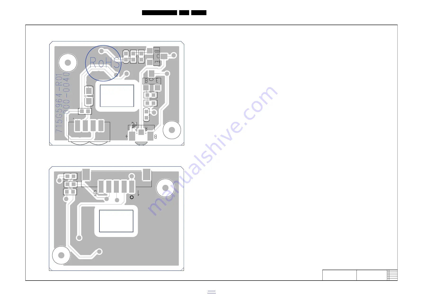
IR/LED board layout
19890_529.eps
715G5964
IR/LED panel
layout top/bottom
2012-10-29
C1
C2
C
3
LED1
Q1
Q2
R1
R5
R6
R7
R8
U1
ZD4
ZD7
CN1
R2
R3
R4
ZD5
ZD8
Layout IR/LED panel (top side)
Layout IR/LED panel (bottom side)


