background image

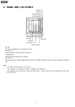
9.1.2. Description of Each Part

LED light (BATALM): Turns on to indicate the dropping of the lithium battery voltage (less than 2.8V).

LED light (SD ACCES): Turns on when the SD card is accessing.

SD card slot: Mounts the system program SD card.

Reset Switch: Press at the system reset.

System Initialize Switch:

On default startup, set the switch to the "SYSTEM INITIALIZE" position for the power ON. Return the switch to the "NORMAL"
position when the main power switch starts to flash. On normal startup, turn the power ON with the "NORMAL" position.

USB connector: B type connector. Used for the PC programming.

PAGING 1, 2: External PAGING output. Connect to the device with the built-in amplifier.

MOH 1, 2: External music on-hold input.

24

KX-TDA100CE

Содержание TDA 100

Страница 1: ... If lead free solder was used in the manufacture of this product the printed circuit boards will be marked PbF Standard leaded Pb solder can be used as usual on boards without the PbF mark When this mark does appear please read and follow the special instructions described in this manual on the use of PbF and how it might be permissible to use Pb solder during service and repair work ORDER NO KMS0...

Страница 2: ...RD CIRCUIT OPERATION 23 9 1 MPR CARD 23 10 BACK BOARD CIRCUIT OPERATION 31 11 TROUBLESHOOTING GUIDE 32 11 1 MPR CARD 32 12 DIAGNOSIS 50 12 1 DIAGNOSIS FEATURES 50 12 2 DIAGNOSIS TEST 54 13 IC DATA 59 13 1 IC101 59 14 TERMINAL GUIDE OF ICS TRANSISTORS AND DIODES 63 15 HOW TO REPLACE A FLAT PACKAGE IC 64 15 1 PREPARATION 64 15 2 PROCEDURE 64 15 3 REMOVING SOLDER FROM BETWEEN PINS 64 16 CABINET AND E...

Страница 3: ...reful not to heat too long PbF solder will tend to splash if it is heated much higher than its melting point approximately 1100 F 600 C If you must use Pb solder on a PCB manufactured using PbF solder remove as much of the original PbF solder as possible and be sure that any remaining is melted prior to applying the Pb solder When applying PbF solder to double layered boards please check the compo...

Страница 4: ...B1 A45 B45 CN107 A1 B1 LED202 LED201 RUN CN201 PSUP1367Z B PSUP1367Z A 3 1 ALM A45 B45 B CN112 C205 R326 R323 R324 R334 R329 R325 R335 R330 R331 R336 R338 C206 CN114 CN113 L104 L105 R312 R318 R340 R342 C204 R311 R313 R306 R303 R302 C209 C210 R348 R345 C207 R347 R344 R343 R346 C208 R305 R304 R301 R307 R308 R314 R315 R309 C201 C203 R317 R316 R310 C202 L106 L110 L111 L112 L107 L109L102 L101 L103 L108...

Страница 5: ... wire 2 Turn on the power switch 3 Measure the resistance value with ohmmeter between the jumpered AC plug and each exposed metal cabinet part such as screw threads control shafts handle brackets etc Note Some exposed parts may be isolated from the chassis by design These will read infinity 4 If the measurement is outside the specified limits there is a possibility of shock hazard The equipment sh...

Страница 6: ...ource port Paging Internal Level Control 6 dB to 3 dB in 3 dB steps External 2 ports Volume Control 15 dB to 15 dB in 1 dB steps Serial Interface Port RS 232C 1 max 115 2 kbps USB 1 Extension Connection Cable SLT 1 pair wire T R DPT 1 pair wire D1 D2 or 2 pair wire T R D1 D2 APT 2 pair wire T R D1 D2 DSS Consoles and Add on Key Module 1 pair wire D1 D2 Dimension KX TDA100 334 mm W x 390 mm H x 270...

Страница 7: ...or Opener 8 1 When only T76xx series and T7560 T7565 DPTs and SLTs are connected If other DPTs or APTs are connected the maximum number will decrease as each of these units is counted as 4 sets of SLTs or DPTs T76xx series and T7560 T7565 4 3 3 Power Supply Unit Selection Hybrid IP PBX needs an optional power supply unit PSU suitable for its configuration Calculate the amount of load figures from ...

Страница 8: ...5 SYSTEM OVERVIEW 5 1 SYSTEM CONFIGURATIONS 8 KX TDA100CE ...

Страница 9: ...CTI Link Card Power Supply Units PSUs KX TDA0104XJ KX TDA0108XJ PSU M PSU S M Type Power Supply Unit S Type Power Supply Unit Cell Stations CS s KX TDA0142CE 4 Channel Cell Station Unit for DECT Portable Station Proprietary Equipment KX A228XJ KX A229XJ S M type Back up Battery Cable L type Back up Battery Cable KX A258XJ Blank Slot Cover KX T30865X Doorphone Available Telephones The Hybrid IP PBX...

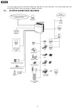
Страница 10: ...upply capacity of the Hybrid IP PBX may differ from the values described in this manual depending on the model number Please consult your dealer for detailed information 5 3 SYSTEM CONNECTION DIAGRAM 10 KX TDA100CE ...

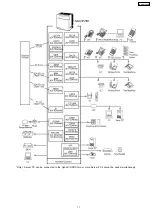
Страница 11: ... Only 1 Server PC can be connected to the Hybrid IP PBX Two or more Server PCs cannot be used simultaneously 11 KX TDA100CE ...

Страница 12: ...C Port They work as system programing administration interface port SMDR information output port computer telephony integration port Note Line capacity of this cabinet is up to 108 ports These limitation of line capacity is checked at installation of slot assignment Line capacity is sum of each card port number except DHLC card In case of DHLC card they are regarded as 8 PITS ports and 8 SLT ports...

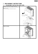
Страница 13: ...ove the Lib by sliding it in the direction of the arrow 1 2 This will be removed if the user attaches the Pad Lock as shown in a Fig 1 3 Loosen the Screw 4 Front Cover is removed in the direction of an arrow 2 5 Loosen the two Screws 6 Remove the MPR Card 13 KX TDA100CE ...

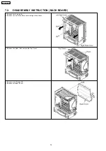
Страница 14: ...SEMBLY INSTRUCTION BACK BOARD 1 Remove four Screws A 2 Remove the Left Side Cover and the Right Side Cover 3 Remove the Hook And remove the Top Cover 4 Remove nine Screws B 5 Remove the Back Cover 14 KX TDA100CE ...

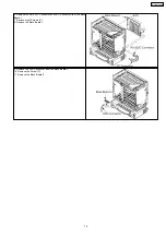
Страница 15: ...232C Connector and LED Connector from the Back Board 1 7 Remove eight Screws C 8 Remove the Back Board 1 9 Remove the LED Connector from the Back Board 2 10 Remove the Screw C 11 Remove the Back Board 2 15 KX TDA100CE ...

Страница 16: ...POWER detects the voltage drop of the AC input and the DC output and transfers it to MPR 8 1 1 MPR Card This card is the main control section of this unit It controls all the cards mounted on the free slots and communication of RS 232C ports The front of the MPR card is equipped with two LEDs LED1 and LED2 that indicate the operating status of this card two rotary switches used to decide a system ...

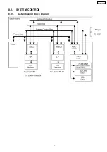
Страница 17: ...8 2 SYSTEM CONTROL 8 2 1 System Control Block Diagram 17 KX TDA100CE ...

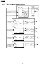
Страница 18: ...8 2 2 Voice TDM Highway Bus Block Diagram 18 KX TDA100CE ...

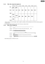
Страница 19: ...mber which is output in accordance with the inserted slot and the time slot are assigned on a software base For the detail of output slot for each card refer to the service manual of card 8 2 4 Back Board Signaling Back board waveform of TDM bus for voice 19 KX TDA100CE ...

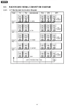
Страница 20: ...8 3 BACK BOARD SIGNAL CONNECTION DIAGRAM 8 3 1 CT Bus System Connection Diagram 20 KX TDA100CE ...

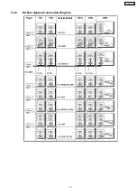
Страница 21: ...8 3 2 EC Bus System Connection Diagram 21 KX TDA100CE ...

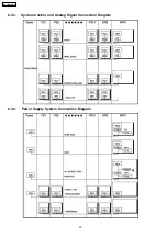
Страница 22: ...8 3 3 System Control and Analog Signal Connection Diagram 8 3 4 Power Supply System Connection Diagram 22 KX TDA100CE ...

Страница 23: ...64Mbit x 2 for work area SRAM 4Mbit x 2 for user data backup SD card I F for operating programs x 1 USB I F for PC programming x 1 MOH External sound input x 2 PAGING External output x 2 Expanded memory connector x 1 Modem card connector x 1 3 Operation Rating Power Input 15V Power Output 15V for MOH 3 3V for I O 3 3VBB back board signal line pull up 3 3VB for SRAM backup 1 8V for CPU core 1 9VB f...

Страница 24: ...ystem reset System Initialize Switch On default startup set the switch to the SYSTEM INITIALIZE position for the power ON Return the switch to the NORMAL position when the main power switch starts to flash On normal startup turn the power ON with the NORMAL position USB connector B type connector Used for the PC programming PAGING 1 2 External PAGING output Connect to the device with the built in ...

Страница 25: ...5 0 ADD0 7 EC_CLK EC_nRST EC_AD 15 0 EC_CBE 1 0 EC_nPAR EC_nFRAME EC_nTRDY EC_nSTOP EC_nPERR EC_nCDET EC_nINT EC_IDSEL H100_bus Regulator 1 8V IC404 Battery 3 0V 3 3VB 3 3VB DC_ALM nIRQ_USB nIRQ_SDB ACALM POWTYPE 1 0 Series Reg CODEC 3 3V 3 3V_BB for B B 3 3V USB Interface ML60852A Termination EC_bus CS Generation for Flash SRAM SDB USB TCXO X103 16 384MHz RMT card Option 3 3V 30pin Connection nPR...

Страница 26: ... 9 1 4 2 Detail of Block Description CPU block Configuration IC101 CPU IC107 reset IC IC103 spread clock IC X101 CPU source clock X102 clocking clock and so on Function IC101 Generates the select signal in accordance with the memory map and operates Readout Storage of data between each peripheral Controls the DMA transfer between USB I F or built in serial controller and memory Operates input outp...

Страница 27: ...Data Bus nDACK0 1 DMA Acknowledge For USB I F DCD2 Data Carrier Detect DCLK_RMT Codec Clock 8MHz For RMT nDC_ALM DC ALARM DC alarm signal Indicates the declined DC voltage L Alarm condition DIN_RMT Codec Data Input For RMT DOUT_RMT Codec Data Output For RMT DQMLL nWE0 DQMLU nWE1 DQMUL nWE2 DQMUU nWE3 Data Input Output Mask Write Enable DQM signal for SDRAM and WE signal for each memory IC and ASIC...

Страница 28: ...PRS_MEX Press MEX Information of MEX Card Attachment L Attached H Not attached nPRS_RMT Press RMT Information of RMT Card Attachment L Attached H Not attached nPRS_SDB Press SD card Information of SD Card Attachment L Attached H Not attached nRAS3L Lower Byte Address Row Address Strobe RAS signal for SDRAM nRAS3U Upper Byte Address Row Address Strobe RAS signal for SDRAM nRD Read USB I F SD card I...

Страница 29: ...USB device and makes data transfer by max 11Mbps DMA function of CPU is utilized to transfer the data SD card block Configuration IC205 SD card I F IC209 X202 20MHz CN211 SD card connector and so on Function Loads the main program and the system data from the SD card connected to CN211 by 10Mbps Restores the system data periodically MOH PAGING block Configuration IC405 IC406 CODEC IC408 IC409 OP A...

Страница 30: ...vention diode D407 and supplied to IC101 clock block power BAT401 which is a lithium battery for memory backup is connected to the power supply of IC301 IC302 SRAM via D408 D409 IC411 compares BAT401 output voltage to the reference voltage about 2 8V and drives LED BATALM that indicates dropping of backup voltage IP401and IP402 block the line respectively when over current flows to 15V and 3 3V li...

Страница 31: ...ly unit to the cards CONNECTORS EXPLANATION 1 Power Supply Unit Connector CN100 2 Free Slot Connectors CN102 CN106 3 Option Card Slot Connector CN107 4 MPR Card Connector CN112 5 RS 232C Connector CN113 CN113 is connected D Sub connector in front of the product 6 LED Connector CN114 CN114 is connected LED Board on the product 31 KX TDA100CE ...

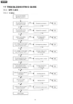
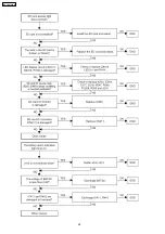
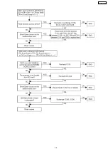
Страница 32: ...11 TROUBLESHOOTING GUIDE 11 1 MPR CARD 11 1 1 Startup 32 KX TDA100CE ...

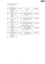
Страница 33: ...33 KX TDA100CE ...

Страница 34: ...34 KX TDA100CE ...

Страница 35: ...35 KX TDA100CE ...

Страница 36: ...36 KX TDA100CE ...

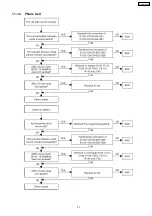
Страница 37: ...11 1 2 Phone Call 37 KX TDA100CE ...

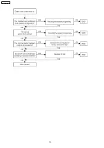
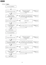
Страница 38: ...11 1 3 Paging 38 KX TDA100CE ...

Страница 39: ...39 KX TDA100CE ...

Страница 40: ...40 KX TDA100CE ...

Страница 41: ...11 1 4 MOH Using 41 KX TDA100CE ...

Страница 42: ...42 KX TDA100CE ...

Страница 43: ...43 KX TDA100CE ...

Страница 44: ...11 1 5 USB Connection 44 KX TDA100CE ...

Страница 45: ...45 KX TDA100CE ...

Страница 46: ...11 1 6 RS 232C Connection 46 KX TDA100CE ...

Страница 47: ...47 KX TDA100CE ...

Страница 48: ...11 1 7 SD Card I F 48 KX TDA100CE ...

Страница 49: ...11 1 8 Other 49 KX TDA100CE ...

Страница 50: ...X 12 1 1 1 Local Loop Back Diagnosis Diagnose by transmission of the data from MPR to Card and doing the Loop back test to return the data to MPR The point to do Loop back is different from the every cards be able to do full diagnosis by Loop back test on the every points Local loop back diagnosis test Primary circuit Primary circuit loop back test Framer IC ST path Analog IC Analog I F loop back ...

Страница 51: ... X X PT loop back diagnosis test channel Cch port xx C channel Port No xx test Dch port xx D channel Port No xx test Bch port xx B channel Port No xx test PT loop back diagnosis test Primary circuit Primary circuit loopback test ASIC PT I F PT I F loopback test Diagnosis result OK PT loop back diagnosis OK NG PT loop back diagnosis NG 12 1 1 5 DSP DTMF Generator Receiver Diagnosis Diagnosis DTMF g...

Страница 52: ...er IC alarm signal detection diagnosis OK NG Framer IC alarm signal detection diagnosis NG 12 1 1 8 Framer IC Error Detection Diagnosis Diagnose the feature to detect the alarm signal of Framer IC is normal action DHLC DLC SLC8 L SLC8 MSLC SLC16 CS INF LCOT T1 E1 BRI PRI OPB3 E M CTI LINK Object of Card X X X Diagnosis point Bipolar violation error Bipolar violation error detection test CRC error ...

Страница 53: ... NG 12 1 1 13 CTI LINK Loop Back Diagnosis Diagnose by Loop back test to CS INF DHLC DLC SLC8 L SLC8 MSLC SLC16 CS INF LCOT T1 E1 BRI PRI OPB3 E M CTI LINK Object of Card X Diagnosis result OK CTI LINK loop back diagnosis OK NG CTI LINK loop back diagnosis NG 12 1 2 Pair Port Test Pair Port Test SUMMARY Description Diagnosis Pair Port Test to pair up inside line and outside line DHLC DLC SLC8 L SL...

Страница 54: ...12 2 DIAGNOSIS TEST 1 Click Diagnosis of Utility 54 KX TDA100CE ...

Страница 55: ...2 Pair Port Test operation Select card for Test 3 Click Pair Port Test 55 KX TDA100CE ...

Страница 56: ...4 Click OK 5 Click Cancel 56 KX TDA100CE ...

Страница 57: ...6 Card Test operation Select card for Test 7 Click Card Test 57 KX TDA100CE ...

Страница 58: ...8 Click OK 9 Click Cancel 58 KX TDA100CE ...

Страница 59: ... IRL3 PTH 3 I External interrupt request input port H 12 IRQ4 PTH 4 I External interrupt request input port H 13 D31 PTB 7 I O Data bus I O port B 14 D30 PTB 6 I O Data bus I O port B 15 D29 PTB 5 I O Data bus I O port B 16 D28 PTB 4 I O Data bus I O port B 17 D27 PTB 3 I O Data bus I O port B 18 D26 PTB 2 I O Data bus I O port B 19 VssQ Power for I O 0V 20 D25 PTB 1 I O Data bus I O port B 21 Vss...

Страница 60: ...59 VssQ Power for I O 3 3V 60 A5 O Address bus 61 A6 O Address bus 62 A7 O Address bus 63 A8 O Address bus 64 A9 O Address bus 65 A10 O Address bus 66 A11 O Address bus 67 A12 O Address bus 68 A13 O Address bus 69 VssQ Power for I O 0V 70 A14 O Address bus 71 VccQ Power for I O 3 3V 72 A15 O Address bus 73 A16 O Address bus 74 A17 O Address bus 75 A18 O Address bus 76 A19 O Address bus 77 A20 O Ad...

Страница 61: ...123 WAIT I Hardware wait request 124 RESETM I Manual reset request 125 ADTRG PTH 2 I Analog trigger input port H 126 IOIS16 PTG 7 I IOIS168 PCMCI I O port G 127 ASEMD0 PTG 6 I ASE mode 4 I O port G 128 ASEBRKAK PTG 5 I O ASE break acknowledge I O port G 129 PTG 4 CKIO2 I O Input port G clock output 130 AUDATA 3 PTG 3 I O I AUD data input port G 131 AUDATA 2 PTG 2 I O I AUD data input port G 132 Vs...

Страница 62: ...rt interruption 180 MCS 4 PTC 4 PINT 4 O I O Mask ROM chip select I O port C port interruption 181 VssQ Power for I O 0V 182 WAKEUP PTD 3 O I O Interrupt request notification on standby mode I O port D 183 VccQ Power for I O 3 3V 184 RESETOUT PTD 2 O I O Reset output I O port D 185 MCS 3 PTC 3 PINT 3 O I O I Mask ROM chip select I O port C port interruption 186 MCS 2 PTC 2 PINT 2 O I O I Mask ROM ...

Страница 63: ...14 TERMINAL GUIDE OF ICS TRANSISTORS AND DIODES 63 KX TDA100CE ...

Страница 64: ...B by temporarily soldering two diagonally opposite pins in the correct positions on the PCB Be certain each pin is located over the correct pad on the PCB 2 Apply flux to all of the pins on the IC 3 Being careful to not unsolder the tack points slide the soldering iron along the tips of the pins while feeding enough solder to the tip so that it flows under the pins as they are heated 15 3 REMOVING...

Страница 65: ...16 CABINET AND ELECTRICAL PARTS LOCATION 65 KX TDA100CE ...

Страница 66: ...16 1 EXTENSION BOARDS FOR SERVICING 66 KX TDA100CE ...

Страница 67: ...17 ACCESSORIES AND PACKING MATERIALS 67 KX TDA100CE ...

Страница 68: ...n Remarks 9 PSMH1205Z CHASSIS LED 10 PSHD1091Z BOLT WITH NUT 11 PSKV1016Z1 COVER RIGHT SIDE ABS HB 12 PSYCTDA100AL COVER FRONT PC ABS 5V 13 PSMD1040Y FRAME LOWER 14 PSMH1230Z FRAME 15 PSMH1222Z ANGLE RS 232C 16 PSMH1206Y ANGLE 17 PSMH1207Z ANGLE 18 PSKK1035Z1 LID PC ABS 5V 19 PSKR1001Y1 GUIDE CABLE PC ABS 5V 20 PSKL1016Z1 STAND ABS HB 21 PSMH1234Z ANGLE FRONT 22 PQHR10379Z CLAMPER 23 PSGB1001Z BAD...

Страница 69: ...1 PSVD1VGCT LED LED103 PSVD1SRCT LED CONNECTORS CN103 K1KA90B00008 CONNECTOR 90P CN205 K1KAC0A00037 CONNECTOR 120P CN206 K1KB30A00117 CONNECTOR 30P CN207 PSJP07A44Z CONNECTOR 7P CN209 K1KB04B00036 CONNECTOR 4P S CN211 K1NA09E00022 CONNECTOR 9P JACKS JK401 PSJJ1D001Z JACK S JK402 PSJJ1D001Z JACK S JK403 PSJJ1D001Z JACK S JK404 PSJJ1D001Z JACK S COMPONENTS PARTS RA101 D1HA1038A005 RESISTOR ARRAY RA1...

Страница 70: ...UV1C104ZFV 0 1 C163 ECUV1C104ZFV 0 1 C166 ECUV1C104ZFV 0 1 C167 ECUV1C104ZFV 0 1 C168 ECUV1H102KBV 0 001 C170 ECUV1C104ZFV 0 1 Ref No Part No Part Name Description Remarks C174 ECUV1C104ZFV 0 1 C201 ECUV1H220JCV 22p C202 PQCUV1A225ZF 2 2 C203 ECUV1H220JCV 22p C204 ECUV1A105ZFV 1 C205 ECUV1C104ZFV 0 1 C206 ECUV1C104ZFV 0 1 C207 ECUV1C104ZFV 0 1 C208 ECUV1C104ZFV 0 1 C209 PQCUV1A225ZF 2 2 C210 ECUV1...

Страница 71: ... 8k R134 ERJ3GEYJ103 10k R135 ERJ3GEY0R00 0 R136 ERJ3GEY0R00 0 Ref No Part No Part Name Description Remarks R137 ERJ3GEYJ103 10k R138 ERJ3GEYJ103 10k R139 ERJ3GEYJ103 10k R140 ERJ3GEYJ330 33 R142 ERJ3GEYJ330 33 R143 ERJ3GEYJ330 33 R144 ERJ3GEYJ470 47 R145 ERJ3GEYJ470 47 R146 ERJ3GEYJ680 68 R148 ERJ3GEYJ103 10k R150 ERJ3GEYJ332 3 3k R151 ERJ3GEYJ332 3 3k R152 ERJ3GEYJ332 3 3k R153 ERJ3GEYJ332 3 3k ...

Страница 72: ...J105 1M R450 ERJ3GEYJ823 82k R451 ERJ3GEYJ823 82k R452 ERJ3GEYJ222 2 2k R453 ERJ3GEYJ223 22k R454 ERJ3GEYJ222 2 2k Ref No Part No Part Name Description Remarks R455 ERJ3GEYJ223 22k R456 ERJ3GEYJ223 22k R457 ERJ3GEYJ223 22k R458 ERJ3GEYJ472 4 7k R459 ERJ3GEYJ472 4 7k R460 ERJ3GEYJ222 2 2k R461 ERJ3GEYJ222 2 2k R462 ERJ3GEYJ473 47k R463 ERJ3GEYJ473 47k R464 ERJ3GEY0R00 0 R465 ERJ3GEY0R00 0 R468 ERJ3...

Страница 73: ...RJ3GEY0R00 0 Ref No Part No Part Name Description Remarks L115 ERJ3GEY0R00 0 L116 ERJ3GEY0R00 0 L117 ERJ3GEY0R00 0 L118 ERJ3GEY0R00 0 L119 ERJ3GEY0R00 0 L120 ERJ3GEY0R00 0 L121 ERJ3GEY0R00 0 L122 ERJ3GEY0R00 0 L123 ERJ3GEY0R00 0 L124 ERJ3GEY0R00 0 L125 ERJ3GEY0R00 0 L126 ERJ3GEY0R00 0 L127 ERJ3GEY0R00 0 L128 ERJ3GEY0R00 0 L129 ERJ3GEY0R00 0 L130 ERJ3GEY0R00 0 L131 ERJ3GEY0R00 0 L132 ERJ3GEY0R00 0 ...

Страница 74: ...TAL OSCILLATORS Ref No Part No Part Name Description Remarks X101 PSVCC0025GT CRYSTAL OSCILLATOR X102 PSVCC0019CT CRYSTAL OSCILLATOR X103 H1B1635B0016 CRYSTAL OSCILLATOR X201 H0J120500019 CRYSTAL OSCILLATOR X202 H0J200500030 CRYSTAL OSCILLATOR OTHERS E1 PQDF996Z SHAFT E2 PQHR10005Z SPACER E3 PQUB14Z2 LEVER PA V0 E4 PSGE1005Z COVER ABS HB E5 PSGE1006Z COVER ABS HB E6 PSHD1088Z SCREW ABS HB E7 PSHE1...

Страница 75: ...0k R200 ERJ3GEYJ103 10k R201 ERJ3GEYJ103 10k R202 ERJ3GEYJ103 10k R343 ERJ3GEYJ103 10k R344 ERJ3GEYJ103 10k R345 ERJ3GEYJ103 10k FILTERS L101 PFVF1A471SG CERAMIC FILTER L102 PFVF1A471SG CERAMIC FILTER L103 PFVF1A471SG CERAMIC FILTER L104 PFVF1A471SG CERAMIC FILTER L105 PFVF1A471SG CERAMIC FILTER L106 PFVF1A471SG CERAMIC FILTER L107 PFVF1A471SG CERAMIC FILTER L108 PFVF1A471SG CERAMIC FILTER L109 PF...

Страница 76: ... DIAGRAM Note 1 DC voltage measurements are taken with an oscilloscope or a tester with a ground 2 The schematic diagrams and circuit board may be modified at any time with the development of new technology 76 KX TDA100CE ...

Страница 77: ...41 TP153 TP138 TP133 TP148 TP132 TP156 TP131 TP146 TP154 TP151 TP155 TP143 TP158 TP159 TP162 TP160 TP157 TP161 TP284 TP274 TP287 TP270 TP280 TP277 TP279 TP272 TP269 TP282 TP285 TP275 TP271 TP276 TP288 TP273 TP268 TP283 TP267 TP291 TP266 TP281 TP289 TP286 TP290 TP278 TP211 TP209 TP210 TP207 TP203 TP201 TP193 TP199 TP205 TP186 TP195 TP214 TP188 TP189 TP208 TP202 TP190 TP191 TP216 TP200 TP187 TP194 T...

Страница 78: ... TP417 3 3V TP421 TP423 TP422 TP420 TP418 TP426 TP430 TP427 TP424 TP431 TP429 TP425 3 3V TP428 TP437 3 3V TP438 TP434 TP439 TP433 TP436 TP432 TP435 TP448 TP449 TP406 3 3V_BB 15VIN HALT HALT DG 3 3V R198 4 7K IC111 14 7 C159 0 1u 3 3V FIL111 1 2 3 DG C160 1 0u TP567 3 3V IC110 14 7 C163 0 1u QA101 1 4 3 2 5 DG TP556 IC110 13 12 IC110 11 10 IC110 3 4 IC110 5 6 TP559 TP570 TP576 TP577 TP578 TP579 TP5...

Страница 79: ... B4 15 B1 18 B3 16 B5 14 A3 4 1 DIR A1 2 A2 3 A4 5 A5 6 B2 17 B7 12 B6 13 A7 8 2G 19 A8 9 B8 11 VCC 20 GND 10 3 3V DG DG 3 3V C215 0 1u C216 0 1u DG DG LA 1 16 J216 0 IC209 11 10 IC209 13 12 DG IC209 14 7 IC209 5 6 IC209 9 8 IC209 3 4 IC209 1 2 X202 20 000MHz C217 15p C218 15p DG TP1020 TP1021 R247 1k R248 1M R249 NC DG FIL208 1 2 3 C219 0 1u 3 3V FIL209 1 2 3 DG C220 1 0u TP1024 TP1022 R250 33 TP...

Страница 80: ...DQ2 5 DQ3 7 DQ4 8 DQ5 10 DQ6 11 DQ7 13 DQ8 74 DQ9 76 DQ10 77 DQ11 79 DQ12 80 DQ13 82 DQ14 83 DQ15 85 DQM0 bit7 0 16 DQM1 bit15 8 71 VCC 43 VCCQ 75 VCCQ 81 NC 30 NC 57 NC 69 NC 70 NC 73 VSSQ 46 VSSQ 52 VSSQ 78 VSSQ 84 VSS 86 VCCQ 3 VCCQ 9 IC306 VCC 1 DQ16 31 VCCQ 35 DQ17 33 DQ18 34 VSSQ 6 DQ19 36 DQ20 37 VCCQ 41 DQ21 39 DQ22 40 VSSQ 12 DQ23 42 VCC 15 DQM2 bit23 16 28 WE 17 CAS 18 RAS 19 CS 20 BA0 2...

Страница 81: ...45 IC409 5 6 7 R459 4 7K 15V TP854 15V IC409 1 2 3 4 8 1 0u C436 10K R447 R457 22K 1M R449 22K R455 TP877 TP852 TP856 TP870 2 2K R454 0 015u C431 0 033u C438 L410 TP864 1000P C440 L412 82K R451 C448 1 0u 10K R443 TP869 TP860 47K R463 DG C428 0 1u TP858 C447 1 0u C434 22u 16V NC R414 2 2K 3 3V VREF VREF VREF VREF VREF D403 10V Q403 E C B R406 1K TP806 D406 4 3V IC120 14 1 7 IC121 14 7 DG DG 3 3VB 5...

Страница 82: ...erve A33 EC_AD 2 CT_D 7 Reserve B33 EC_nSTOP CT_D 3 CT_D 1 EC_nCDET TXD2 EC_nTRDY CT_D 0 EC_nINT RXD2 EC_nPERR Reserve B31 EC_AD 15 Reserve A35 EC_AD 1 Reserve A31 Reserve A32 EC_AD 14 EC_AD 0 EC_AD 13 EC_nRST CT_D 2 EC_AD 12 EC_nCBE 1 EC_AD 11 EC_nCBE 0 Reserve B35 EC_AD 10 EC_PAR CT_D 4 EC_AD 9 EC_nFRAME Reserve B36 EC_AD 8 CT_D 5 EC_AD 7 TXD2 POWTYPE 1 Reserve A33 AC_ALM Reserve A32 EC_AD 6 CT_...

Страница 83: ...AD 6 CT_D 1 EC_AD 4 EC_nCDET EC_AD 2 EC_AD 15 EC_AD 0 EC_AD 13 EC_PAR EC_AD 11 Reserve B31 EC_nPERR EC_AD 9 Reserve A31 EC_AD 7 EC_nSTOP EC_AD 5 nHALT EC_AD 3 RINGER EC_AD 1 30V EC_nRST nFAN_ALM EC_nCBE 1 nBATT DIAG_R RINGER_AC POWTYPE 0 Reserve B35 DC_ALM Reserve A35 nLOS Reserve A35 Reserve A33 EC_AD 12 DC_ALM POWTYPE 1 Reserve B32 Reserve B35 TXD2 EC_AD 14 EC_AD 13 POWTYPE 0 Reserve B33 EC_AD 0...

Страница 84: ...201 2 2u CN113 1 2 3 4 5 6 7 8 9 L104 L105 L106 L107 L108 L109 L110 L111 L101 L102 L103 CN114 1 2 3 CN201 1 2 3 LED201 Green 1 2 LED202 Red 1 2 L112 EC_CLK EC_nTRDY EC_nFRAME EC_nCBE 0 EC_AD 11 EC_nPERR EC_PAR EC_AD 0 EC_AD 2 EC_AD 4 EC_AD 6 EC_AD 8 EC_AD 10 EC_AD 12 EC_AD 14 EC_nINT CT_D 0 CT_D 2 CT_D 4 CT_D 6 CT_NETREF CT_FRAME TXD1 CS1 DR1 DC_ALM POWTYPE 0 DIAG_R EC_nCBE 1 EC_nRST EC_AD 1 EC_AD...

Страница 85: ...36MHz 16 384MHz Switching the frequency of 20Hz 25Hz is possible by the soft setting The abobe mentioned waveform is the example of 20Hz Switching the pulse spacing of 2976msec 3840msec 4992msec 5120msec is possible by the soft setting The abobe mentioned waveform is the example of 5120msec KX TDA100CE 85 ...

Страница 86: ...Waveform 7 Waveform 8 20MHz 12MHz KX TDA100CE 86 ...

Страница 87: ...04 J305 J306 J307 J308 120 R193 R192 J301 R504 R194 J330 IP401 16 1 8 9 IC127 1 7 8 14 C402 IC413 1 4 5 8 D407 CN206 1 29 30 2 C454 J309 J311 J310 J312 L301 R553 L149 L151 L152 L154 L148 L150 R197 L153 L155 L156 L158 L160 L162 L157 L159 CN205 C167 1 R560 IC102 180 121 R561 2 119 120 C166 C453 Q411 R401 J328 R503 J303 J302 SDIN INIT NORM JK404 MOH 1 JK401 PAGE 2 X101 C129 C459 C460 R471 FIL403 FIL4...

Страница 88: ... C219 J116 IC107 BATALM RA203 C211 C209 J222 FIL207 FIL208 FIL209 IC209 14 8 7 1 L227 R250 R249 J216 J227 L228 J224 J321 WP ACC R303 R302 J323 SDCLK J214 J217 C314 C316 86 44 10 11 1 20 1 10 20 IC208 11 IC306 1 43 J106 J110 C108 C107 C130 C134 C133 C131 J153 C111 R112 R509 FIL201 L229 J226 C202 C204 C205 USBCLK R108 R123 R121 R119 FIL104 C106 J152 C101 J109 C105 FIL101 FIL105 OFF SW106 ON L103 XTA...

Страница 89: ... L110 L111 L112 L107 L109 L102 L101 L103 L108 9 1 3 1 R333 R332 R337 R328 R327 R206 C105 R202 R147 R149 R158 R151 R148 R150 R159 R152 R153 R160 R162 R155 R154 R161 R172 R166 R167 R173 R175 R169 R168 R174 R176 R170 R177 R183 R185 R179 R178 R184 R186 R180 R181 R187 R194 R189 R182 R188 R195 C106 R197 C108 R192 R193 R198 R103 R101 R102 R104 C107 R111 R105 R106 R112 R113 R107 R108 R114 R109 R115 R205 R...

Страница 90: ...EC_nSTOP GND EC_nPERR EC_PAR EC_nCBE 1 EC_nRST GND GND EC_AD 1 EC_AD 3 EC_AD 5 EC_AD 7 EC_AD 9 EC_AD 11 EC_AD 13 EC_AD 15 EC_nCDET nSHW_FH CT_D 1 CT_D 3 CT_D 5 CT_D 7 CT_C8 nLOS GND Reserved Reserved Reserved Reserved Reserved M nS 30V RING_SYNC RING_SIN 3 3V AC_ALM POWTYPE 1 DIAG_T RINGER_AC nLUHW 1 MASTER nS nSHW_CLK 15VPT 40V Power GND EC_CLK GND EC_nTRDY EC_nFRAME EC_nCBE 0 EC_AD 5 GND GND EC_...

Страница 91: ...91 KX TDA100CE A KXTDA100CE ...

Отзывы: