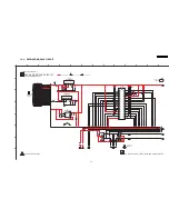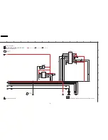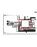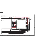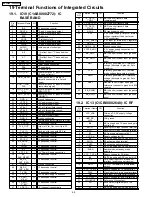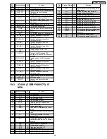
Pin
NO.
Terminal Name
I/O
Function
24
CP_OUT
O
PLL charge pump output.
25
VCC_CP
-
Supply voltage for PLL charge pump.
26
GND_CP
-
Charge pump circuit ground
connection
27
VCC_XTAL
-
Supply voltage for Crystal Oscillator.
28
XTAL
I
Crystal and load capacitor C1
connection or Reference Clock input.
29
GND_XTAL
-
Crystal and load capacitor gnd
connection
30
VCC_VCO
-
Supply voltage for VCO1/VCO2.
31
GND_VCO
-
VCO ground connection.
32
TUNE
I
VCO frequency tuning control voltage
input.
33
BYPASS
-
VCO bypass
34
B4
I
RX/TX base band AGC control bit 4.
35
RX_BB_Q-
O
Receiver baseband Q negative
differential output.
36
O
Receiver baseband Q positive
differential output.
37
RX_BB_I-
O
Receiver baseband I positive
differential output.
38
O
Receiver baseband I negative
differential output.
39
VCC_RX_
VGA
-
Supply voltage for RX VGA.
40
RX_HP
I
Receiver I and Q channel AC
coupling high-pass corner frequency
selection.
41
VCC_RX_FL
-
Supply voltage for RX Baseband
filter.
42
TX_BB_Q-
I
Transmit baseband Q negative
differential input.
43
I
Transmit baseband Q positive
differential input.
44
TX_BB_I-
I
Transmit baseband I negative
differential input.
45
I
Transmit baseband I positive
differential input.
46
VCC_RX_MX
-
Supply voltage for RX downconverter
47
ANT_SEL
-
GND connection
48
CPRXTX
I
Transmit and Receiver mode
selection
19.3. IC1000 (C2BBYY000375): IC
MCU
Pin
NO.
Terminal Name
I/O
Function
1
P2.1
-
No Connection
2
P2.0
O
Port 2 (mode: LDO)
3
P0.1
O
Port 0 (mode: LINK)
4
P0.0
O
Port 0 (mode: PCONT)
5
P12.0
I
Potential input for external low-
voltage detection
6
RST
I
System reset input
7
FLMD0
-
Flash memory programming mode
setting
8
EXCLK
I
External clock input for main system
clock
9
X1
-
Connecting resonator for main
system clock
10
REGC
-
Connecting regulator output (2.5 V)
stabilization capacitance for internal
operation
11
VSS
-
Ground potential connection
12
VDD
-
Positive power supply
13
P6.0
I/O Clock input/output for I
2
C
14
P6.1
I/O Serial data I/O for I
2
C
15
P3.3
I
External interrupt request input
16
P3.2
I
External interrupt request input
Pin
NO.
Terminal Name
I/O
Function
17
P3.1
I
Connection for on-chip debug mode
setting pins
18
P3.0
I
External interrupt request input
19
P1.7
I
External count clock input
20
P1.6
O
External interrupt request input
21
P1.5
-
No Connection
22
P1.4
I
Serial data input to UART6
23
P1.3
O
Serial data output from UART6
24
P1.2
O
Serial data output from CSI10
25
P1.1
I
Serial data input to UART0
26
P1.0
O
Serial data output from UART0
27
AVREF
-
A/D converter reference voltage input
28
AVSS
-
A/D converter ground potential
connection
29
P2.3
I
A/D converter analog input
30
P2.2
I
A/D converter analog input port 2
69
SH-FX85P / SH-FX85PC
Содержание SH-FX85P
Страница 12: ...7 4 Digital Receiver Operations as stand alone audio amplifier SB FX85 12 SH FX85P SH FX85PC ...
Страница 39: ...11 2 Checking of D Amp and D Port P C B 39 SH FX85P SH FX85PC ...
Страница 41: ...12 1 3 PANEL P C B 4GH 0Q 1 2 56 0 5 2 2 2 0 2 2 0 2 3 3 3 3 3 41 SH FX85P SH FX85PC ...
Страница 42: ...12 2 Waveform Chart RF TEST POINT PLAY 42 SH FX85P SH FX85PC ...
Страница 44: ...SH FX85P SH FX85PC 44 ...
Страница 48: ...SH FX85P SH FX85PC 48 ...
Страница 50: ...50 SH FX85P SH FX85PC ...
Страница 66: ...SH FX85P SH FX85PC 66 ...
Страница 70: ...70 SH FX85P SH FX85PC ...
Страница 71: ...20 Exploded Views 20 1 Cabinet Parts Location SH FX85P SH FX85PC 71 ...
Страница 72: ...20 2 Packaging SH FX85P SH FX85PC 72 ...

