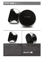
manualshive.com logo in svg
background image

l

General

Power Source:

AC 110V-127V/ 220V-240V,
50/ 60Hz

Power consumption:

155 W

Dimensions (W×H×D):

430×70×439.2 mm

Mass:

5 kg

l

Amplifier section

RMS Output Power: Dolby Digital Mode

l

Total RMS Dolby Digital

mode Power:

1000 W

At 1kHz and total harmonic of 10%

l

Front:

90 W/ Channel (4

)

l

Center:

320 W/ Channel (4

)

l

Surround:

90 W/ Channel (4

)

At 100Hz and total harmonic of 10%

l

Subwoofer:

320 W/ Channel (4

)

PMPO Output Power:

7500W

DIN Output Power: Dolby Digital Mode

l

Total DIN Dolby Digital

mode Power

740 W

At 1kHz and total harmonic of 1%

l

Front:

65 W/ Channel (4

)

l

Center:

240 W/ Channel (4

)

©

2006 Panasonic AVC Networks Singapore Pte.

Ltd. All rights reserved. Unauthorized copying and
distribution is a violation of law.

SA-HT740GCP

Colour
(S).......................Silver Type

l

Surround:

65 W/ Channel (4

)

At 100Hz and total harmonic of 1%

l

Subwoofer:

240 W/ Channel (4

)

DIN Output Power Stereo Mode

l

Total DIN Stereo mode

Power

360 W

At 1kHz and total harmonic of 1%

l

Front:

60 W/ Channel (4

)

At 100Hz and total harmonic of 1%

l

Subwoofer:

240 W/ Channel (4

)

l

Preset Memory

FM 15 stations

AM/ MW 15 stations

l

FM tuner section (FM)

Frequency Range:

87.5-108.0MHz

(50kHz step)

Sensitivity:

2.5µV (IHF)

S/N 26dB

2.2µV

Antenna Terminals:

75

(unbalanced)

l

AM tuner section (AM/MW)

Frequency Range:

522-1629kHz (9kHz step)

520-1630kHz (10kHz step)

AM Sensitivity S/N 20dB at
999kHz:

560µV/m

DVD Home Theater Sound System

Specifications

ORDER NO.MD0605182C3

Содержание SA-HT740GCP

Страница 1: ... AVC Networks Singapore Pte Ltd All rights reserved Unauthorized copying and distribution is a violation of law SA HT740GCP Colour S Silver Type lSurround 65 W Channel 4Ω At 100Hz and total harmonic of 1 lSubwoofer 240 W Channel 4Ω DIN Output Power Stereo Mode lTotal DIN Stereo mode Power 360 W At 1kHz and total harmonic of 1 lFront 60 W Channel 4Ω At 100Hz and total harmonic of 1 lSubwoofer 240 W...

Страница 2: ...udio output DISC Number of channels 5 1 ch FL FR C SL SR SW Audio performance Frequency response DVD linear audio 4 Hz 22 kHz 48 kHz sampling 4 Hz 44 kHz 96 kHz sampling DVD Audio 4 Hz 88 kHz 192 kHz sampling CD Audio 4 Hz 20 kHz S N ratio CD Audio 105 dB Dynamic range DVD linear audio 95 dB CD Audio 95 dB Total harmonic distortion CD Audio 0 005 lVideo section Video system Signal system NTSC Comp...

Страница 3: ...osis and special mode setting 19 9 1 Service Mode Summary Table 19 9 2 Service Mode Table 19 9 3 DVD Self Diagnostic Function Error Code 24 9 4 Sales Demonstration Lock Function 26 9 5 Service Precautions 26 10 Assembling and Disassembling 28 10 1 Disassembly Flow Chart 29 10 2 Main Components and P C B Locations 30 10 3 Disassembling the Top Cabinet 31 10 4 Disassembling the Front Panel Assembly ...

Страница 4: ...am 55 19 Schematic Diagram Notes 61 20 Schematic Diagram 63 20 1 A Optical Pickup Unit HDMI Module Circuit 63 20 2 B Main Circuit 70 20 3 C Power AC inlet Sub power Voltage Selector Circuit 75 20 4 D FL Headphone Loading Motor Tray Motor Sensor Regulator Circuit 78 21 Printed Circuit Board 81 21 1 A HDMI Module P C B 81 21 2 B Main AC inlet Sub Power P C B 82 21 3 C Power P C B 83 21 4 E FL Headph...

Страница 5: ...ct a 1 5kΩ 10 watts resistor in parallel with a 0 15µF capacitors between each exposed metallic part on the set and a good earth ground such as a water pipe as shown in Figure 1 3 Use an AC voltmeter with 1000 ohms volt or more sensitivity to measure the potential across the resistor 4 Check each exposed metallic part and measure the voltage at each point 5 Reverse the AC plug in the AC outlet and...

Страница 6: ...arth ground Alternatively obtain and wear a commercially available discharging ESD wrist strap which should be removed for potential shock reasons prior to applying power to the unit under test 2 After removing an electrical assembly equipped with ES devices place the assembly on a conductive surface such as aluminum foil to prevent electrostatic charge buildup or exposure of the assembly 3 Use on...

Страница 7: ...7 SA HT740GCP ...

Страница 8: ...t look directly into the pick up lens 2 Do not use optical instruments to look at the pick up lens 3 Do not adjust the preset variable resistor on the pickup lens 4 Do not disassemble the optical pick up unit 5 If the optical pick up is replaced use the manufacturer s specified replacement pick up only 6 Use of control or adjustments or performance of procedures other than those specified herein m...

Страница 9: ...ork using Lead Free Solder PbF The lead free solder has to be used when repairing the equipment for which the lead free solder is used Definition The letter of PbF is printed on the PCB using the lead free solder To put lead free solder it should be well molten and mixed with the original lead free solder Remove the remaining lead free solder on the PCB cleanly for soldering of the new IC Since th...

Страница 10: ...able of the optical pickup unit removed should be short circuited with a short pin or a clip 3 The flexible cable may be cut off if an excessive force is applied to it Use caution when handling the flexible cable 4 The antistatic FPC is connected to the new optical pickup unit After replacing the optical pickup unit and connecting the flexible cable cut off the antistatic FPC 5 2 Grounding for ele...

Страница 11: ...11 SA HT740GCP ...

Страница 12: ...Remote control AM loop antenna FM indoor antenna Video Cable Screws AC cord Speaker cable Speaker label Power plug adaptor 6 Accessories 12 SA HT740GCP ...

Страница 13: ...T SLEEP FL DISPLAY ZOOM SETUP LEVEL Frame by frame Select or register menu items on the television screen Show on screen menu Select television channels Return to previous screen Adjust the volume of the main unit Change the television s video input mode Adjust the television volume Display current playback condition Turn the unit on off Select disc s title numbers etc Enter numbers Basic operatio...

Страница 14: ...xt disc tray Open Close the disc drawer 5 DISC SELECTOR Select the disc tray TUNE MODE FM MODE Stop playing Select the tuning mode Adjust the FM reception condition MEMORY Play discs Memorize the receiving radio stations TUNING Skip or slow search play Select the radio stations Standby on switch POWER MUSIC PORT OPEN CLOSE I Press to switch the unit from on to standby mode or vice versa In standby...

Страница 15: ... 1 DVD RW DVD R CD R RW DVD RW Discs recorded and finalized on DVD video recorders or DVD video cameras 1 2 Discs reco Finalize the disc after recording 2 Discs recorded and finalized This unit can play CD R RW recorded with the above formats Close the sessions or finalize This unit also plays HighMAT discs recording HDCD encoded CDs sound better because they are encoded with 20 bits as compared w...

Страница 16: ...of digits and should be done in the order you want to play them this may not work at times Files must have the extension Extension WMA or wma Compatible compression rate between 48 kbps and 320 kbps You cannot play WMA files that are copy protected This unit does not support Multiple Bit Rate MBR Extension MP3 or mp3 Compatible compression rate between 32 kbps and 320 kbps This unit does not suppo...

Страница 17: ...8 New Features 8 1 About HDMI 8 1 1 What is HDMI 8 1 2 Advanced Digital Pictures 17 SA HT740GCP ...

Страница 18: ...8 1 3 Advanced Digital Sound 8 1 4 Easy to Use 8 1 5 HDMI Compatible Products 18 SA HT740GCP ...

Страница 19: ...re version check Initialization of the player factory setting is restored Used after replacement of micro computer FLASH ROM IC EEPROM and HDMI module ENTER DVD module reset During initialisation FUNCTIONS DVD laser drive current check Refer to the section 9 2 4 Optical Pick up Self Diagnosis 3 CD laser drive current check PAUSE Writing of laser drive current value after replacement of optical pic...

Страница 20: ... 0 x DAXX is expressed DVDnn UXX Error code 0 x DBXX is expressed DVDnn HXX Error code 0 x DXXX is expressed DVDnn FXXX Error code 0 x 0000 is expressed DVDnn F xx denotes the error code In STOP no disc mode press STOP button on the player and PAUSE button on the remote control unit Initial setting of laser drive current Initial current value for each of DVD laser and CD laser is separately saved ...

Страница 21: ... unit In STOP no disc mode press STOP button on the player and 8 button on the remote control unit Initialization User settings are cancelled and player is initialized to factory setting Cancelled automatically 5 seconds later Displays frequency of communication errors between system control IC and mechanism control IC during DVD module Communication error display DVD Module Reset To reset DVD Mod...

Страница 22: ...operation timer Shown to the left is DVD laser time and to the right is CD laser time Time is shown in 4 digits of decimal notation in a unit of 10 hours 0000 will follow 9999 Time is shown in 5 digits of decimal notation in a unit of 10 hours 00000 will follow 99999 FL Display Key Operation Front Key Item Description Mode Name Shown to the left is DVD laser time and to the right is CD laser time ...

Страница 23: ...Note Press FL DISPLAY button on remote control Note Press FL DISPLAY button on remote control unit for next page display unit for next page display 23 23 23 23 23 34 34 34 34 34 23 SA HT740GCP ...

Страница 24: ...s n STOP on main unit for next error F500 DSC error DSC IC8251 stops in the occurrence of servo error startup focus error etc Press n STOP on main unit for next error F501 DSC not Ready error DSC system computer communication error Communication failure caused by idling of DSC Press n STOP on main unit for next error F502 DSC Time out error Similar as F500 Press n STOP on main unit for next error ...

Страница 25: ...lation during highlight display Press n STOP on main unit for next error F4FF Force initialize failure time out Timeout when force initialization fails Press n STOP on main unit for next error F700 MBX overflow When replying message to disc manager Press n STOP on main unit for next error F701 Message command does not end Next message is sent before replying to disc manager Press n STOP on main un...

Страница 26: ...the disc eject function LOCKED is displayed on the unit and ordinary operation is disabled 9 4 1 Setting Prohibiting removal of disc 1 Select the DVD CD function 2 Press and hold down the button and the power button on the player for at least three seconds The message ___LOCKED_ appears when the function is activated Note OPEN CLOSE DISC CHECK and DISC CHANGE buttons are invalid and the player dis...

Страница 27: ...o be done or not Selection of Yes No 4 a If Yes is selected version updating is performed b If No is selected only recovery is performed 5 a When updating is finished remove the disc according to the message appearing on the screen b Remove the disc according to the message appearing on the screen 6 Turn off the power Note If the AC power supply is shut out during version up due to a power failure...

Страница 28: ...ecks or replacement are required Disassembling the Top Cabinet Disassembling the Front Panel Disassembling the Tray Assembly Disassembling the Rear Panel Disassembling the Mechanism Base Block Disassembling the FL Head phone P C B Disassembling the HDMI Module P C B Disassembling the Regulator P C B Disassembling the Main P C B Disassembling the AC Inlet Power Sub power Voltage Selector P C B Disa...

Страница 29: ...10 1 Disassembly Flow Chart 29 SA HT740GCP ...

Страница 30: ...10 2 Main Components and P C B Locations 30 SA HT740GCP ...

Страница 31: ...4 Keep the open lock gear pressed in anti clockwise direction and push back the tray assembly Step 5 Detach the FFC cables from connectors CN5705 CN5707 CN2013 Step 6 Release the claws of the front panel in the directions Step 7 Detach the front panel assembly in the direction of arrow 10 5 Disassembling the Tray Assembly Follow Step 1 to Step 7 of Item 10 4 Step 1 Press and hold the open lock gea...

Страница 32: ...tep 1 Remove 2 screws on each side of the mechanism base block Caution Take note of the screw type used During assembling use the correct screw type and at the correct location Step 2 Detach FFC cable at connector CN2005 Step 3 Detach FFC cables at connectors FP8251 FP8531 Step 4 Remove the mechanism base block 10 8 Disassembling the FL Head phone P C B Follow Step 1 to Step 7 of Item 10 4 Disasse...

Страница 33: ...ted 10 11 Disassembling the Main P C B Follow Step 1 to Step 4 of Item 10 6 Follow Step 1 to Step 4 of Item 10 7 Step 1 Remove 3 screws and 2 screw covers Step 2 Remove the shield plate Step 3 Remove the tab Step 4 Detach the FFC cables from connectors CN2011 CN5701 CN5708 CN2001 Step 5 Remove the Main P C B 10 12 Disassembling the AC Inlet Power Sub Power Voltage Selector P C B Follow Step 1 to S...

Страница 34: ...llow Step 1 to Step 7 of Item 10 12 Step 1 Desolder all pins of D5711 D5716 D5717 D5718 Step 2 Desolder 2 pins of Regulator IC Step 3 Remove the Regulator IC Note Refer to the diagrams of Power P C B Section 20 3 for location of the parts 10 15 Disassembly of Switch Regulator IC IC5701 Follow Step 1 to Step 7 of Item 10 12 Step 1 Desolder all pins of IC5701 Step 2 Desolder 2 pins of Switch Regulat...

Страница 35: ...R in the direction of arrow 10 17 Disassembly of the Rotary Tray Follow Step 1 to Step 3 of Item 10 5 Step 1 Remove tray screw and tray spring Step 2 Remove rotary tray 10 17 1 Disassembly of the Open Lock Gear Step 1 Rotate open lock gear in the direction of arrow Anti clockwise Step 2 Release claw of open lock gear remove open lock gear in the direction of arrow 35 SA HT740GCP ...

Страница 36: ... 1 to Step 3 of Item 10 5 Step 1 Remove 2 screws Step 2 Release 4 claws at Tray Motor P C B and Sensor P C B 10 18 Disassembly of the Traverse Unit Follow the Item 10 7 Step 1 Rotate cam gear anti clockwise Align at position A as marking on gear with arrow Step 2 Flip the base mecha unit in vertical position Step 3 Press upward a push backward b and press to left c to release CD traverse unit 10 1...

Страница 37: ...ve Loading Motor P C B 10 18 3 Disassembly of the Drive Gear A B Step 1 Release the claw in the direction of arrow 1 and then push drive gear shaft up Step 2 Remove Drive Gear A and Drive Gear B 10 18 4 Disassembly of Fixed Plate Magnet and Clamper Release 3 claws in the direction of arrow 10 18 5 Disassembly of Cam Gear Support Piece Step 1 Rotate A in cam gear anti clockwise 37 SA HT740GCP ...

Страница 38: ... Step 1 Press the claw and push the Slide Plate L up Step 2 Remove slide plate L R and change lever as arrow shown 10 19 Assembly of Tray Assembly Step 1 Rotate cam gear anti clockwise Align at position C as marking on gear with arrow Step 2 Make sure drive gear A at vertical position 38 SA HT740GCP ...

Страница 39: ...Step 3 Push tray assembly to the direction of arrow shown 39 SA HT740GCP ...

Страница 40: ...ct all the cables Step 4 Connect 2 fans Step 5 Turn over Power P C B Main P C B HDMI module P C B FL P C B Head phone P C B and Voltage Selector P C B Step 6 Position mechanism base block and tray assembly in horizontally Step 7 Connect the AC cord and switch on the power Step 8 Insert CD into tray assembly Step 9 Press DISC SELECTOR button to lock the CD For example press 1 of 5 DISC SELECTOR if ...

Страница 41: ...justment if there is a noticeable degradation in picture quality Optical adjustments cannot be made inside the optical pickup Adjustment is generally unnecessary after replacing the traverse unit 13 2 2 Important points in electrical adjustment Follow the adjustment procedures described in this manual 13 3 Storing and handling of test discs Surface precision is vital for DVD test discs Be sure to ...

Страница 42: ...ind the optimum point 3 Finish the procedure with tilt adjustment Jitter value depends on the model 1 If the jitter value changes like B the optimum point is easy to find 2 If the jitter value changes like A set the optimum point near the middle 13 4 1 3 Check after adjustment Play test disc or any other disc to make sure there is no picture degradation in the inner middle and outer peripheries an...

Страница 43: ... OUT SIGNAL DATA REQUEST DATA RESPONSE DIGITAL SERVO CONTROLLER DATA SLICE LOOP FILTER DIGITAL VIDEO DISC INITIAL LOGO ABBREVIATIONS E EC ECR ENCSEL ETMCLK ETSCLK ERROR TORQUE CONTROL ERROR TORQUE CONTROL REFERENCE ENCODER SELECT EXTERNAL M CLOCK 81MHz 40 5MHz EXTERNAL S CLOCK 54MHz F FBAL FCLK FE FFI FEO FG FSC FSCK FOCUS BALANCE FRAME CLOCK FOCUS ERROR FOCUS ERROR AMP INVERTED INPUT FOCUS ERROR ...

Страница 44: ...SERIAL SUB CODE CLOCK SUB CODE Q DATA SYSTEM CLOCK T TE TIBAL TID TIN TIP TIS TPSN TPSO TPSP TRCRS TRON TRSON TRACKING ERROR BALANCE CONTROL BALANCE OUTPUT 1 BALANCE INPUT BALANCE INPUT BALANCE OUTPUT 2 OP AMP INPUT OP AMP OUTPUT OP AMP INVERTED INPUT TRACK CROSS SIGNAL TRACKING ON TRAVERSE SERVO ON INITIAL LOGO ABBREVIATIONS V VBLANK VCC VCDCONT VDD VFB VREF VSS V BLANKING COLLECTOR POWER SUPPLY ...

Страница 45: ...9 1 Ref No MODE 1 2 3 4 5 6 7 8 9 10 11 12 13 14 15 16 17 18 19 20 CD PLAY 0 1 0 1 3 4 0 1 0 1 0 1 0 1 3 4 3 4 0 1 0 1 0 1 0 1 0 1 0 1 0 1 0 1 0 1 3 4 0 1 Ref No MODE 21 22 23 24 25 26 27 28 29 30 31 32 33 34 35 36 37 38 39 40 CD PLAY 0 1 3 4 1 3 1 3 1 3 1 3 1 2 1 2 1 2 1 2 1 3 1 3 1 3 0 1 0 1 1 2 1 3 1 3 0 1 1 3 Ref No MODE 41 42 43 44 45 46 47 48 49 50 51 52 53 54 55 56 57 58 59 60 CD PLAY 0 1 0...

Страница 46: ... 2 6 2 1 5 0 0 2 5 2 5 2 5 0 Ref No MODE 1 2 3 4 CD PLAY 3 3 1 2 0 1 0 1 Ref No MODE 1 2 3 4 5 CD PLAY 3 4 3 4 0 1 0 1 Ref No MODE 1 2 3 4 5 6 7 8 CD PLAY 0 1 0 1 0 1 0 1 3 3 3 3 0 1 3 4 Ref No MODE 1 2 3 4 5 6 7 8 9 10 11 12 13 14 15 16 17 18 19 20 CD PLAY 0 1 3 4 3 4 3 4 3 4 3 4 3 4 3 4 0 1 0 1 3 4 3 4 3 4 3 4 1 0 0 1 0 1 3 4 3 4 3 4 Ref No MODE 21 22 23 24 25 26 27 28 29 30 31 32 33 34 35 36 37...

Страница 47: ...PLAY 0 0 1 0 0 6 9 6 9 0 0 0 1 0 0 0 0 0 0 0 1 0 0 STANDBY 0 0 0 0 6 9 6 9 0 0 0 0 0 0 0 0 0 0 0 0 Ref No MODE 1 2 3 4 5 6 7 8 CD PLAY 0 1 0 1 0 1 6 9 0 0 0 6 9 STANDBY 0 0 0 6 9 0 0 0 6 9 Ref No MODE 1 2 3 4 5 6 7 8 9 10 11 12 13 14 CD PLAY 0 0 0 6 9 0 0 0 0 0 0 6 9 0 0 0 STANDBY 0 0 0 6 9 0 0 0 0 0 0 6 9 0 0 0 Ref No MODE 1 2 3 4 5 6 7 8 9 10 11 12 13 14 15 16 17 18 19 20 CD PLAY 4 9 0 0 2 1 4 7...

Страница 48: ... 0 0 Ref No Q5701 Q5702 Q5703 MODE E C B E C B E C B E C B E C B CD PLAY 7 9 11 0 7 9 0 6 3 1 3 5 4 3 4 2 3 4 4 2 4 0 0 1 3 2 0 4 STANDBY 8 0 11 0 7 9 0 6 3 1 3 5 4 3 4 1 3 4 4 2 4 1 0 3 2 0 4 Ref No MODE E C B E C B E C B E C B E C B CD PLAY 17 5 17 0 16 8 0 3 8 0 6 5 18 1 7 0 0 4 9 0 0 0 1 0 7 STANDBY 17 5 16 9 16 8 0 3 8 0 6 5 18 1 7 0 0 4 9 0 0 0 1 0 7 Ref No MODE E C B 1 2 3 4 E C B E C B CD ...

Страница 49: ...2 5 1 2 0 1 0 STANDBY 0 1 0 4 8 0 0 4 0 2 4 8 0 Q9101 Q9102 Ref No MODE 1 2 3 4 CD PLAY 3 7 2 5 0 0 2 STANDBY 0 2 0 4 0 4 7 Q9103 Ref No MODE 1 2 3 4 CD PLAY 3 7 2 5 0 0 2 STANDBY 0 2 0 4 0 4 7 Q9103 Ref No MODE 1 2 3 1 2 3 12 1 0 9 1 12 7 0 9 1 4 CD PLAY 3 7 2 5 0 0 2 STANDBY 0 2 0 4 0 4 7 IC2901 IC2902 Sensor P C B Regulator P C B Tray Motor P C B Loading Motor P C B 49 SA HT740GCP ...

Страница 50: ... PLAY 100Vp p 500nsec div WF No IC5001 36 PLAY 96Vp p 500nsec div WF No IC2001 12 PLAY 5 4Vp p 100nsec div WF No IC2102 20 PLAY 0 1Vp p 500usec div WF No IC2102 30 PLAY 4 4Vp p 5msec div WF No IC2103 7 PLAY 1 2Vp p 500usec div WF No IC2801 18 PLAY 1 1Vp p 20usec div 1Vp p 20usec div 0 5Vp p 20usec div WF No IC2801 21 PLAY 0 9Vp p 20usec div WF No IC2801 24 PLAY 2 2Vp p 20usec div WF No IC2801 30 P...

Страница 51: ...BBA000163 10p C3EBEG000073 8p C3EBGC000055 8p C0HBB0000057 44p C1AB00002239 80p C1BB00001098 100p RFKWMHA0L160 B1GFGCAA0001 B1BACG000048 Cathode A Ca Anode Anode Cathode Ca A A Ca Cathode Anode MN864701 164p MN2DS0009AP 256p MN101C49GHF1 100p 1 24 25 48 C0AABB000125 C0DABYY00002 1 4 8 5 3 1 1 2 4 3 4 2 5 3 UNR511V00L UNR521100L B0ADCJ000020 B0ACCK000005 B0JCAE000001 B0BC2R4A0006 B0BC4R0A0006 B0BC3...

Страница 52: ...SA HT740GCP 52 ...

Страница 53: ...710 P5701 110V 127V 220V 240V 50 60HZ AC IN 1 6 CN5705 CN5707 CN5712 CN5713 1 2 8 1 2 18 14 1 19 9 14 1 PbF PbF PbF PbF PbF PbF PbF PbF PbF A HDMI MODULE P C B SIDE A TO SPINDLE MOTOR ASS Y TO TUNER PACK UNIT TO WIRELESS MAIN P C B B POWER P C B C VOLTAGE SELECTOR P C B L AC INLET P C B D SUB POWER P C B E FL P C B F HEADPHONE P C B G LOADING MOTOR P C B H TRAY MOTOR P C B I SENSOR P C B J TO OPTI...

Страница 54: ...SA HT740GCP 54 ...

Страница 55: ...LPC1 LPC01 VIN9 VIN10 VIN5 VIN6 VIN7 VIN8 VIN4 VIN3 VIN2 VIN1 MOTOR SPINDLE MOTOR TRAVERSE ACT F HFM ACT F ACT T ACT T ACTUATOR COIL FOCUS COIL TRACKING BIAS2 TRACKING COIL FOCUS COIL TRAVERSE SPINDLE MOTOR DRIVE C0GBG0000048 IC8251 PWM1 VHALF TRV DRV 144 128 MUTE12 MUTE CH4 20 MUTE4 MUTE3 LDIN 6 OPOUT SHIFT LEVEL SHIFT LEVEL SHIFT LEVEL SHIFT LEVEL IC8001 MN2DS0009AP DV3 2 LSI LD DRIVE LD DRIVE 1...

Страница 56: ... 48 49 50 51 58 59 60 61 62 63 64 18 A0 1 8 18 25 DATA DQ15 DQ0 45 43 41 39 36 34 32 30 44 42 40 35 38 33 31 29 223 225 221 227 228 229 38 16 17 18 19 208 210 212 216 217 213 211 209 207 203 201 199 206 202 198 230 237 232 238 240 242 244 246 247 245 200 243 241 53 51 50 48 47 45 44 42 13 11 10 8 7 5 4 2 35 22 34 33 32 31 30 29 26 25 24 23 SA HT740GCP BLOCK DIAGRAM CR PR R SR CK LR CK AD OUT1 AD O...

Страница 57: ...DING IC2003 C0GAG0000007 MOTOR DRIVE TRAY IC5750 B B CONTROL DRIVE CONTROL DRIVE INTERRUPTOR PHOTO Q9103 B TU SCL FM DET TU SD TU SDA ST DO DVD STA DVD CMD DVD CK 36 40 38 37 39 43 42 44 CL CE SD DI ST DO DVD STAT DVD CMD DVD CLK S VIDEO OUT JK2001 IC2801 VIDEO BUFFER C9ZB00000461 GND 10 VCC 1 B B VIDEO OUT JK2001 CR BLUE JK2001 CB GREEN JK2001 Y RED JK2001 BIAS 6dB LPF 6 MHz CLAMP 6dB LPF 6 MHz L...

Страница 58: ...SEL OUT SRSEL OUT CSEL OUT SUBSEL OUT 13 22 14 21 53 52 AMP IC5010 INVERTER CLOCK GENARATOR C0JBAB000472 X5010 14 1 5 6 2 4 8 10 9 11 3 28 19 20 21 22 26 27 15 16 24 BIT AUDIO DIGITAL TO ANALOG CONVERTER C0FBBK000050 DVD MIX L DVD MIX R DVD FL DVD FR DVD SL DVD SR DVD CNT SUBW QR8420 Q2006 MUTING SCK MD MC MS DATA1 DATA4 DATA3 DATA2 LRCK MANAGER CLOCK SYSTEM CLOCK SYSTEM ZERO DETECT ZFLAG 5 BCK SR...

Страница 59: ... STANDBY V OUT2 IN 2 1 3 9 7 13 25 22 2 6 17 49 48 40 41 36 34 30 32 D5041 Q5001 5002 Q5095 5096 Q5031 16 23 IN 1 CLK IN 1 2 MUTE_5 6 MUTE_3 MUTING Q2911 2914 V OUT2 V OUT1 V OUT1 B Q5022 Q5023 Q5025 2 13 1 14 3 12 1 12 14 13 15 11 _ MUSIC PORT AMP IC2105 1 MUSIC PORT SELECTOR C0JBAR000326 IC2906 4 5 9 2 6 3 10 MOD DA 64 MUTE F 66 MUTE C SELECT A 68 51 WIRELSS Rch CN2003 5V VM DETECT ID SET JK6801...

Страница 60: ...0 5742 Q5744 FAN MOTOR DRIVE 9V REGULATOR C0DAZYY00001 C0DAZYY00001 OUT IN 3 1 9V REGULATOR IC5702 OUT IN 3 1 2 3 1 SWITCHING REGULATOR OUT IN 2 1 M SWITCHING Q2901 Q2909 DC DETECT Q5908 D5903 REGULATOR B IC5705 12V REGULATOR C0CAAYG00011 B Q5751 SWITCHING B Q5702 SWITCHING Q5701 CURRENT LIMMITTING SWITCH Q5747 SWITCHING PC5701 FEED BACK 2 1 3 _ DIFFERENTIAL AMP IC5703 1 5 7 6 _ DC DETECT AMP C0AB...

Страница 61: ...ltage values depending on the internal impedance of the DC circuit tester Important safety notice Components identified by mark have special characteristics important for safety Furthermore special parts which have purposes of fire retardant resistors high quality sound capacitors low noise resistors etc are used When replacing any of components be sure to use only manufacturer s specified parts s...

Страница 62: ...62 SA HT740GCP ...

Страница 63: ...05 L2 J0JCC0000307 C6 22P C8 0 1 C7 0 1 T F F T HFM TA TB TD TC FE2 FE1 GND IM GND IM RF VREF2 RF PIN DVD LD CD LD GND LD DVD GND OEIC VREF1 VCC SUB2 SUB1 PIN CD SUBSEL GND VCC GND GND OUT GND GND TB TA TC TD FE1 FE2 IM RF GND VREF VCC SUB2 SUB1 SW LD CD LD DVD LDGND OPTICAL PICKUP UNIT CIRCUIT C4 0 22 C5 22P L3 J0JBC0000105 R2 0 R4 0 C2 0 1 C1 0 1 C3 0 1 R1 0 R3 0 R5 0 R6 0 R7 6 8K VR2 6 8K VR1 6...

Страница 64: ...0J1050018 FL8421 F1H0J1050018 FL8102 F1H0J1050018 IC8151 C0DBEHG00006 QR8420 UNR521100L IC8691 C0JBAA000346 IC8695 C0JBAA000346 QR8111 XP0621400L IC8421 COFBBK000050 IC8111 C0DBZYY00018 FL8101 F1H0J1050018 R8421 0 C8051 10 NRST HDMIRST P13 FL8104 F1J1E1040022 DMIXOUT LRCK SRCK AOUT0 AOUT1 AOUT2 DMIXOUT STBDAC OP_CPU_STAT OP_CPU STAT OP_CPU_CLK OP_CPU CLK GND VCC GND VCC SBT3 SBO3 MSEL ZERO1 MS MC ...

Страница 65: ..._5 MDQ_6 MDQ_7 MDQ_7 MDQ_8 MDQ_6 MDQ_9 MDQ_5 MDQ_10 MDQ_4 MDQ_11 MDQ_3 MDQ_12 MDQ_2 MDQ_13 MDQ_1 MDQ_14 MDQ_0 MDQ_15 c7 c8 c6 c9 c5 c10 c4 c11 c3 c12 c2 c13 C1 C14 C0 C15 VDD LDQM WE CAS RAS CS BA0 BA1 DQM0 DQM1 WE CAS RAS CS BA0 BA1 BA1 NCSM BA0 NRAS NCAS DQM1 DQM0 A10 AP A0 A1 A5 A4 MA_11 MA_9 MA_8 MA_7 MA_6 MA_5 MA_4 MA_3 MA_2 MA_5 MA_1 MA_6 MA_4 MA_0 MA_7 MA_10 MA_8 MA_9 MA_11 a3 a2 a5 a1 a6 a...

Страница 66: ... DRV0 DRV1 DRV2 DRV3 DRV4 DRV5 FG NRST VDD12 VSS P14 P13 P12 P11 P10 P9 P8 P7 P6 P5 P4 P3 VDD33 VSS P2 P1 DRV0 DRV1 DRV2 DRV3 DRV4 DRV5 FG P14 P13 P12 P11 P10 P4 P3 P2 P1 MDQ19 TRCDATA2 TRCDATA3 TRCST VSS VDD33 DQM15 DQM0 DQM14 DQM1 DQM13 DQM2 VDD33 VSS MDQ12 MDQ3 MDQ11 MDQ4 MDQ10 MDQ5 MDQ9 MDQ6 VDD33 VSS MDQ8 MDQ7 VDD12 DQM0 DQM1 NWE VSS MCK VDD33 MCKI VSS NCAS NRAS NCSM MA11 BA0 MA9 VSS VDD12 BA...

Страница 67: ...C8232 0 1 C8532 220P C8531 100P C8572 0 1 C8571 10 C8530 0 1 C8533 0 1 C8251 6 3V 220 C8252 0 1 C8564 10 C8561 0 1 C8551 0 1 R8321 68 R8322 0 R8564 22 R8561 0 R8551 0 R8568 47K R8331 68 R8332 0 R8335 68 Q8561 2SD1819A0L LD DRIVE LD DRIVE LD DRIVE LD DRIVE Q8562 B1ADGB000008 R8563 1K R8566 56 R8565 2 2 C8225 1000P C8221 1000P C8226 1000P C8222 820P R8341 68 RX8691 D1H410320002 RX8001 D1H410320002 S...

Страница 68: ...VDD15 VDD33 DO20 DO19 DO18 VSS DO17 DO16 DO15 VDD33 DO14 DO13 DO12 VSS DO11 DO10 DO9 VDD33 DO8 DO7 DO6 VDD15 VSS DO5 DO4 DO3 VDD33 DO2 HPD DO0 VSS AMDAM AMSDI0 AMSDI1 AMSDI2 AMSDI3 VSS AMRX LPSA5 LPSA6 LPSA7 VDD15 PDWN NIRQ HSCL HSDA VSS VDD33 HCLK HCLKDIV0 HCLKDIV1 NTEST SCANTEST VSS TESTM0 TESTM1 TESTM2 MINTEST NRESET VDD15 SOM0 SOM1 ESDA ESCL TMS TCK TDI TDO TRST VSS TESTIN0 TESTIN1 C3710 10 C3...

Страница 69: ...CGND CVCC18 INT HPD DSDA DSCL NC GND CN VIN D 5V D 2 7V LB3902 J0JHC0000045 LB3904 J0JCC0000119 LB3905 J0JCC0000119 LB3906 J0JCC0000119 R3904 4 7K R3905 2K R3906 4 7K C3956 10 C3954 0 1 R3907 2 2K D S G D S G LB3901 J0JHC0000045 C3901 4V 330P C3902 4V 330P NC NC CONT IC3782 C0CBCAD00082 1 8V DC DC CONVERTER 8 7 2 1 6 3 5 4 R3780 1 5K R3781 1 5K R3911 1K RX3902 D1H410120001 VA3909 EZJZ0V800AA L3903...

Страница 70: ... R2295 6 8K R2196 33K R2173 47K R2273 47K R2195 6 8K R2628 10K 1 2 15 16 3 14 4 13 5 12 6 11 7 10 8 9 1 2 31 32 3 30 4 29 5 28 6 27 7 26 8 25 9 24 10 23 11 22 12 21 13 20 14 19 15 18 16 17 1 2 13 14 3 12 4 11 5 10 6 9 7 8 C2191 100P R2197 68K C2621 0 1 R2629 10K C2838 0 1 C2835 25V22 C2806 6 3V100 C2812 0 1 C2810 0 01 C2819 100P C2817 1 C2821 100P C2811 0 1 C2822 100P C2620 100P C2837 0 1 C2834 25...

Страница 71: ..._DET ASP_DA ASP_CK HP_MUTE RMT HOTPLG CEC_IN PULSE SYNC PWM AM_BP TU_SCL SYS6V TU_SDA TU_SD TU_ST RDS DET DVD_CMD DVD_STA DVD_CK MUTE_DVD ROLE_CHG MPORT_DET ASP_DA ASP_CK N C VDD N C TURN_REW TURN_FWD LOAD_FWD VSS LOAD_REV JOG_LED JOG_B JOG_A FL_DAT FL_CK N C FLD_STB N C N C N C WS_LED DISC1_LED DC_DET TURN_REW TURN_FWD LOAD_FWD LOAD_REV JOG_LED JOG_B JOG_A FL_DAT FL_CLK FL_STB WIDESURRLED DISC1_L...

Страница 72: ...1 2K R2610 56K R2402 27K C2401 47 C2301 47 R2214 15K C2217 0 1 C2218 0 1 C2119 1 C2121 0 1 C2221 0 1 C2219 1 C2603 1 C2605 0 47 C2503 0 082 C2502 0 033 R2403 4 7K R2630 0 R2612 68K R2609 1 2K R2625 1 8K R2621 39K R2603 10K R2604 10K R2601 33K R2404 12K R2298 0 R2443 0 R2198 0 R2444 2 2K R2513 2 2K R2635 2 2K R2344 2 2K R2304 12K R2620 56K R2605 12K R2627 68K R2608 56K C2303 0 1 C2403 0 1 C2612 330...

Страница 73: ...0V1 FLVOLOUT d FLFIN HP LCH HP RCH FRVOLOUT FRFIN R2268 2 2K C2270 50V1 C2278 100P C2279 47P R2276 56K C2294 2200P R2275 5 6K C2277 50V1 R2289 1K C2180 0 1 R2277 22 R2279 22 R2193 27 R2293 27 R2278 22 R2280 22 R2281 4 7K C2281 1000P C2280 0 1 4 5 6 1 2 3 R2170 2 2K Q2101 B1GFGCAA0001 IC2103 C0AABB000125 W2025 0 W2024 0 MAIN SIGNAL LINE SA HT740GCP MAIN CIRCUIT MUTING HEADPHONES AMP DUAL OP AMP B S...

Страница 74: ... 10K R2937 470 R2905 3 9K IC2903 C0DAAMH00012 Q2904 B1AAKD000012 C2945 0 01 C2922 6 3V820P C2946 16V100 R2939 39K C2902 0 01 R2918 10K R2921 470 R2925 1 5 R2935 4 7K R2936 180 R2946 33 R2927 1 5 R2920 4 7K STBY VCC OUT GND INV C2919 100P R2919 1K C2920 0 01 R2907 2 7K R2908 560 L2902 G0A101ZA0028 L2903 G0A200D00002 C2930 1 C2926 0 1 C2923 16V100 C2968 16V100 C2969 16V100 C2952 0 01 C2901 25V1000 C...

Страница 75: ...14 0 R5615 0 R5410 220 R5038 220K R5039 220K R5037 47K R5041 0 02 R5042 0 02 R5613 0 R5077 0 R5072 2 7K R5073 22K R5071 0 R5074 4 7K R5627 8 2K C5020 0 1 R5070 4 7K R5487 22 C5230 100P C5113 0 68 C5130 100P C5115 0 68 C5181 0 1 R5181 22 R5110 5 6K R5504 47K C5183 0 1 R5183 22 R5109 5 6K C5386 0 1 R5411 5 6K R5311 5 6K C5406 0 47 R5208 220 R5107 220 R5502 2 2K D5041 B0ACCK000005 R5506 22K C5603 50V...

Страница 76: ...765 22K R5763 2 2K R5793 0 R5766 1 8K R5714 5 6K R5741 1K D5771 B0BC01200019 R5715 15K R5735 0 R5799 1 R5789 10K R5738 15K R5712 2 2K R5729 1 5K R5775 10K R5717 4 7K R5730 82K R5722 10K R5782 5 6K R5720 10K R5710 10K R5711 22 R5706 33K R5707 33K D5702 B0ZAZ0000052 R5709 2 2K R5708 3 3K R5719 10K PC5701 B3PBA0000402 Q5745 B3PBA0000402 R5718 100K R5783 5 6K R5704 0 68 R5788 10K R5703 680 R5731 5 6K ...

Страница 77: ...16V220 C5800 16V220 C5715 16V47 C5729 50V22 C5707 400V 330 C5700 400V 330 C5772 1000P C5725 50V2 2 R5724 1 2K R5753 330 L5750 J0JBC0000015 ZJ5701 1 2 3 ZJ5703 ZJ5702 L5752 J0JBC0000015 L5753 J0JBC0000015 PWM DISC_SENS 20V AM_BP PCONT SYNC SYS6V DC_DET 30_VDD VCC CN5701 CN5702 GND VCC DC_DET SYS6V SYNC DC_GND DC_GND SW SVGND DC 13V DC 13V AM_BP PCONT TRV TRV DGND PHOTO_DRIVER DGND DISC_SENSOR DGND ...

Страница 78: ...902 KEY1 DGND FLGND VREF RMT F F SW 5V_2 FL_IC_IN FL_IC_CLK FL_IC_STB VP WIDE_LED NC NC NC NC NC RMT KEY1 Z6900 B3MAZ0000023 REMOTE SENSOR C6911 0 01 C6917 100P C6916 100p C6919 100p C6929 0 01 WIDE_LED S6900 POWER C6910 6 3V100 C6913 50V3 3 C6201 0 047 C6801 0 1 C6806 100P C6805 100P C6922 0 01 C6928 0 1 C6101 0 047 S6907 SELECTOR INPUT STOP FORWARD BACKWARD PLAY R6812 1 8K R6960 2 2K R6802 2 7K ...

Страница 79: ...LOADING_SW LOAD S9001 M9001 LOADING MOTOR Q9001 CN9003 LOADING MOTOR CIRCUIT Q9102 B3NAA0000102 PHOTO INTERRUPTOR Q9103 B3NAB0000027 PHOTO INTERRUPTOR Q9001 B3NAA0000098 CAM SENSOR T O POWER SMPS CN5702 ON SCHEMATIC CIRCUIT DIAGRAM 15 T O MAIN CIRCUIT CN2005 ON SCHEMATIC DIAGRAM 8 Q9101 B3NAA0000082 POSITION SENSOR C B SA HT740GCP LOADING MOTOR TRAY MOTOR SENSOR REGULATOR CIRCUIT A B C D E F G H 1...

Страница 80: ...SA HT740GCP 80 ...

Страница 81: ...57 LB8530 RX8532 LB8551 LB8561 L8550 C3931 C8023 RX8001 RX8691 R8003 R8601 C8008 RX8611 C8007 C8022 C8020 C8019 C8018 C8001 C8424 LB8691 LB8693 LB8692 C8695 C8691 LB8690 LB8491 R8420 LB8424 LB8431 LB8429 LB8428 LB8427 LB8426 LB8425 LB8422 LB8421 LB8302 LB8301 LB8305 LB8304 LB8303 K8331 K8341 K8335 K8321 K8325 C8422 C8427 C8428 C8426 R8421 RX8111 C8111 R8326 R8401 RX8402 RX8401 RX8403 C8301 L8301 L...

Страница 82: ...2974 R2976 R2023 R2022 R2080 R2021 R2018 R2016 R2015 R2975 R2017 R2019 W2760 W2757 W2604 W2507 W2022 W2605 R2004 R2005 L2002 L2001 L2003 W2121 R2084 C2001 C2008 C2009 C2004 R2003 C2002 W2511 R2002 R2001 Q2003 Q2001 Q2095 W2753 W2316 R2062 D2935 D2005 D2001 D2934 D2002 D2008 D2007 W2119 FP2000 2A CN2007 H2010 IC2901 IC2003 X2001 IC2004 CN2001 IC2105 IC2103 CN2013 R2994 Q2308 Q2307 Q2310 Q2309 IC210...

Страница 83: ...01 C5201 C5101 R5208 R5107 R5056 W4332 R5052 R5011 C5011 C5914 C5016 C5017 C5015 D5013 D5772 D5725 D5010 D5740 D5744 D5743 D5750 D5751 L5750 D5773 C5754 C5756 D5726 D5746 C5738 D5752 C5757 W4104 R5742 R5789 R5743 W4102 W4101 W4009 C5764 C5722 R5722 R5719 R5720 R5721R5732 R5775 R5796 R5747 R5746 D5771 R5741 R5744 R5745 C5721 W4007 R5801 R5788 R5810 R5804 R5803 R5805 D5712 D5714 R5777 R5771 R5728 R5...

Страница 84: ...POWER L6905 L6904 R6949 W6948 W6947 W6919 W6920 W6946 R6922 R6947 R6946 R6957 R6934 W6942 W6941 W6930 W6927 W6931 W6929 W6928 W6926 C6911 C6909 W6925 W6922 C6917 R6917 C6916 C6925 R6914 R6916 L6903 R6927 W6900 W6902 D6910 R6935 R6918 W6901 R6940 C6906 C6919 IC6901 FL6901 R6939 C6904 R6928 W6945 W6943 Q6901 R6948 R6950 R6923 R6924 R6925 R6926 C6923 C6920 R6951 C6921 C6924 D6906 S6804 R6812 R6805 R6...

Страница 85: ...eck laser drive circuitry voltages and current Check CD laser drive Compare the above with OK condition Module Compare the above with OK condition Module Check DVD laser drive Check voltages and LD current and compare with Check voltages and LD current and compare with OK Module OK Module a Check SDRAM address and data bus signal b Check video signals c Check audio DAC circuitry signals Traverse u...

Страница 86: ...lity condition FL display shows U702 U703 1 Check setting of the set in Setup Menu whether HDMI video output is turned ON IC3952 Pin 4 P3901 Problems Checking Points Checking components 5 HDMI got no audio output 1 Audio Data Lines RX8403 RX8402 Check f for s solder s short an and or signal c condition component m component missing damaged as well as d as well as 3 Picture shown on TV not clear sh...

Страница 87: ...Det PCON F F SYNC Wireless IC5001 JK2001 S video Composite Component Head Phone Video Buffer Tuner Pack FM AM Headphone Amp System Control Loading Mechanism Control Block EEPROM Display Driver FL Display Regulator DC Det Motor Drive AC IN and Transformer Power supply control AC Speaker subwoofer Terminal For Speaker Power Amp Power Amp ASP SA HT740 87 SA HT740GCP ...

Страница 88: ...ystem DVD System LSI FEP EFM Demodulate ECC BEP MPEG2 Decode SP Motor TRV Motor IC8611 TRV sw CD DVD IC8251 IC8001 IC8051 IC8421 IC3701 IC8651 Driver FO TR Act TRV SP Motor OPU LD Drive LD Drive EEPROM M M SD RAM SD RAM Flash ROM Flash ROM IC3901 Audio DAC HDMI 88 SA HT740GCP ...

Страница 89: ...n MUSIC PORT In AUX In TUNER In DVD Module HDMI ON ON DVD Mix L R DVD Front L R Volume DVD Center DVD Sub Woofer DVD Surround L R AGC ASS IC2103 DVD 5 1ch Play Back Mode IC2102 H P Amp Head Phone Front L R Center Sub Woofer Surround L R IC5001 HIC ASP 89 SA HT740GCP ...

Страница 90: ...Line Out TCR In AUX In TUNER In DVD Module HDMI ON DVD Mix L R DVD Front L R Volume DVD Center DVD Sub Woofer DVD Surround L R AGC ASS IC2103 2ch Analog input Mode IC2102 H P Amp Head Phone ASP Front L R Center Sub Woofer Surround L R IC5001 HIC 90 SA HT740GCP ...

Страница 91: ...AMP LOGIC SWITCH IC5001 Q2906 Q2907 Q2903 D2902 30V VCC 30V F F VP 12V 7V REG IC2903 IC2908 IC2907 IC2902 IC2901 Q2935 D2912 Q2904 D2915 D2934 SYS 6V IC2301 IC2003 IC2104 IC2205 IC2905 IC2904 FOR WIRELESS MODELS ONLY DVD MODULE IC2102 C 9V C 9V RF 5V IC2103 REG VCC T 9V C 9V MUTING DVD PCONT HIC SECTION SW 5V DAMP 5V 13V M 9V TUNER FL DISPALY MAIN POWER ON MODE AC INPUT ON 91 SA HT740GCP ...

Страница 92: ...02 IC5703 Q5726 RECTIFIER RECTIFIER RECTIFIER RECTIFIER BACKUP T5701 T5721 D5711 D5717 50V 30V VCC 30V VCC 20V SENSE SENSE VCC_CONT SENSE VDD D5716 D5701 IC5701 IC5721 D5705 SYS6V To FL Display F F RECTIFIER SWITCHING CONTROL PC5721 AC POWER TRANSFORMER SUB TRANSFORMER 92 SA HT740GCP ...

Страница 93: ...ET I Rear M Port detect 48 ASP_DA O ASP data R2S15203FP 49 ASP_CK O ASP clock R2S15203FP Pin No Terminal Name I O Function 50 MUTE_HP O Headphone mute 51 MP_SEL SELECT _A O Select front MPort or rear MPort 52 SUB_ LIMITER O Subwoofer frequency Limiter 53 VMUTE O Video mute control 54 N C No connection 55 WIDE_ SURR O Surround Enhancer 56 CEC_OUT I Output port for HDMI 57 WS_EN I Surround Enhancer ...

Страница 94: ...25 Exploded Views 25 1 Cabinet Parts Location 94 SA HT740GCP ...

Страница 95: ...95 SA HT740GCP ...

Страница 96: ...96 SA HT740GCP ...

Страница 97: ...25 2 Packaging 97 SA HT740GCP ...

Страница 98: ...acity values are in microfarads µF unless specified otherwise P Pico farads pF F Farads F Resistance values are in ohms unless specified otherwise 1K 1 000 OHM 1M 1 000K OHM The parenthesized indications in the Remarks columns specify the model names and areas Refer to the cover page The marking RTL indicates the retention time is limited for this item After the discontinuation of this assembly in...

Страница 99: ...MNX0192 VOLTAGE SELECTOR INSULATOR M 64 RXQX0034 SHIELD PLATE UNIT B M TRAVERSE DECK 301 RDG0567 PULSE GEAR M 302 RDG0568 OPEN LOCK GEAR M 303 RDG0569 1 CLOSE LOCK GEAR M 304 RDV0073 TRAY BELT M 305 REZ1734 FFC WIRE M Ref No Part No Part Name Description Remarks 306 RGQ0446 K TRAY BASE M 307 RGQ0359 K1 ROTARY TRAY M 308 RMM0254 2 SLIDE PLATE R M 309 RMB0842 TRAY SPRING M 310 RME0384 CLOSE LOCK GEA...

Страница 100: ...176 TRANSISTOR M Q2914 B1ADCF000001 TRANSISTOR M Q2935 B1BACG000023 TRANSISTOR M Q2936 B1GBCFJN0033 TRANSISTOR M Q3901 2SD1819A0L TRANSISTOR M Q3902 B1CFHA000002 TRANSISTOR M Q3903 B1CFHA000002 TRANSISTOR M Q5001 B1ABCF000011 TRANSISTOR M Q5002 B1ABCF000011 TRANSISTOR M Ref No Part No Part Name Description Remarks Q5014 B1ABCF000011 TRANSISTOR M Q5015 B1ADBL000010 TRANSISTOR M Q5022 B1ABCF000011 T...

Страница 101: ...000042 CHIP BEAD M Ref No Part No Part Name Description Remarks LB8305 J0JBC0000042 CHIP BEAD M LB8401 J0JBC0000042 CHIP BEAD M LB8421 ERJ2GE0R00X CHIP JUMPER M LB8422 ERJ2GE0R00X CHIP JUMPER M LB8423 ERJ2GE0R00X CHIP JUMPER M LB8424 ERJ2GE0R00X CHIP JUMPER M LB8425 ERJ2GE0R00X CHIP JUMPER M LB8426 ERJ2GE0R00X CHIP JUMPER M LB8427 ERJ2GE0R00X CHIP JUMPER M LB8428 ERJ2GE0R00X CHIP JUMPER M LB8429 E...

Страница 102: ...15 CHIP INDUCTOR M L5751 J0JKB0000020 EMI BEAD CORE M L5752 J0JBC0000015 CHIP INDUCTOR M L5753 J0JBC0000015 CHIP INDUCTOR M L6101 J0JBC0000019 CHIP INDUCTOR M L6102 G0C330KA0065 COIL M L6201 J0JBC0000019 CHIP INDUCTOR M L6202 G0C330KA0065 COIL M L6801 J0JBC0000019 CHIP INDUCTOR M Ref No Part No Part Name Description Remarks L6903 J0JBC0000041 CHIP INDUCTOR M L6904 J0JBC0000019 CHIP INDUCTOR M L690...

Страница 103: ...51 ERJ3GEYJ103V 10K 1 16W M R2052 ERJ3GEYJ221V 220 1 16W M R2053 ERJ3GEYJ221V 220 1 16W M R2054 ERJ3GEYJ221V 220 1 16W M R2055 ERJ3GEYJ221V 220 1 16W M R2057 ERJ3GEYJ221V 220 1 16W M R2058 ERJ3GEYJ221V 220 1 16W M R2059 ERJ3GEYJ221V 220 1 16W M R2060 ERJ3GEYJ221V 220 1 16W M R2061 ERJ3GEYJ473V 47K 1 16W M R2062 ERJ3GEYJ221V 220 1 16W M R2063 ERJ3GEYJ221V 220 1 16W M R2064 ERJ3GEYJ103V 10K 1 16W M ...

Страница 104: ...J683V 68K 1 16W M R2617 ERJ3GEYJ682V 6 8K 1 16W M R2619 ERJ3GEYJ123V 12K 1 16W M R2620 ERJ3GEYJ563V 56K 1 16W M Ref No Part No Part Name Description Remarks R2621 ERJ3GEYJ393V 39K 1 16W M R2622 ERJ3GEY0R00V 0 1 16W M R2623 ERJ3GEYJ563V 56K 1 16W M R2624 ERJ3GEYJ273V 27K 1 16W M R2625 ERJ3GEYJ182V 1 8K 1 16W M R2626 ERJ3GEYJ683V 68K 1 16W M R2627 ERJ3GEYJ683V 68K 1 16W M R2628 ERJ3GEYJ103V 10K 1 16...

Страница 105: ...K 1 16W M R5110 ERJ3GEYJ562V 5 6K 1 16W M R5181 ERJ1TYJ220U 22 1W M Ref No Part No Part Name Description Remarks R5183 ERJ1TYJ220U 22 1W M R5189 ERJ3GEYJ823V 82K 1 16W M R5197 ERJ3GEYJ103V 10K 1 16W M R5208 ERJ3GEYJ221V 220 1 16W M R5309 ERJ3GEYJ221V 220 1 16W M R5311 ERJ3GEYJ562V 5 6K 1 16W M R5386 ERJ1TYJ220U 22 1W M R5391 ERJ3GEYJ683V 68K 1 16W M R5410 ERJ3GEYJ221V 220 1 16W M R5411 ERJ3GEYJ562...

Страница 106: ...5932 ERJ3GEYJ103V 10K 1 16W M R5933 ERJ3GEYJ562V 5 6K 1 16W M R5934 ERJ3GEYJ103V 10K 1 16W M R6801 ERJ3GEYJ472V 4 7K 1 16W M R6802 ERJ3GEYJ272V 2 7K 1 16W M Ref No Part No Part Name Description Remarks R6803 ERJ3GEYJ122V 1 2K 1 16W M R6804 ERJ3GEYJ102V 1K 1 16W M R6805 ERJ3GEYJ102V 1K 1 16W M R6807 ERJ3GEYJ223V 22K 1 16W M R6809 ERJ3GEYJ223V 22K 1 16W M R6810 ERJ3GEYJ682V 6 8K 1 16W M R6812 ERJ3GE...

Страница 107: ... JUMPER M Ref No Part No Part Name Description Remarks W2030 ERJ6GEY0R00V CHIP RESISTOR M W2031 ERJ6GEY0R00V CHIP RESISTOR M W2037 ERX2SJ1R5E RESISTOR M W2042 ERJ6GEY0R00V CHIP RESISTOR M W2051 ERJ3GEY0R00V CHIP JUMPER M W2060 ERJ3GEY0R00V CHIP JUMPER M W2061 ERJ6GEY0R00V CHIP RESISTOR M W2072 ERJ3GEY0R00V CHIP JUMPER M W2073 ERJ3GEY0R00V CHIP JUMPER M W2074 ERJ3GEY0R00V CHIP JUMPER M W2075 ERJ6GE...

Страница 108: ...UMPER M K8325 ERJ2GE0R00X CHIP JUMPER M K8331 ERJ2GE0R00X CHIP JUMPER M K8335 ERJ2GE0R00X CHIP JUMPER M K8341 ERJ2GE0R00X CHIP JUMPER M CAPACITORS C2001 ECEA1CKS470I 47 16V M Ref No Part No Part Name Description Remarks C2002 ECJ1VB1C104K 0 1 16V M C2003 ECEA1EKS220B 22 25V M C2004 ECJ1VB1H103K 0 01 50V M C2006 ECEA1HKS2R2B 2 2 50V M C2007 ECJ1VB1C104K 0 1 16V M C2008 ECEA0JKS101B 100 6 3V M C2009...

Страница 109: ...00 6 3V M C2807 ECJ1VB1H103K 0 01 50V M C2808 ECA1AAD221XI 220 10V M C2809 ECEA1EKS220B 22 25V M Ref No Part No Part Name Description Remarks C2810 ECJ1VB1H103K 0 01 50V M C2811 ECJ1VB1C104K 0 1 16V M C2812 ECJ1VB1C104K 0 1 16V M C2814 ECEA1EKS220B 22 25V M C2815 ECEA1EKS220B 22 25V M C2816 ECEA1EKS220B 22 25V M C2817 ECJ1VB1A105K 1 10V M C2818 ECJ1VB1A105K 1 10V M C2819 ECJ1VC1H101J 100P 50V M C2...

Страница 110: ...50 47 63V M C5030 F2A1J470A050 47 63V M C5031 ECEA1HKA100B 10 50V M C5033 ECJ1VB1H104K 0 1 50V M Ref No Part No Part Name Description Remarks C5035 ECJ1VB1H104K 0 1 50V M C5036 ECJ1VB1H104K 0 1 50V M C5040 ECJ1VB1H104K 0 1 50V M C5062 ECA1CAK100XB 10 16V M C5063 ECA1CAK100XB 10 16V M C5066 ECJ1VB1H102K 1000P 50V M C5067 ECJ1VB1H102K 1000P 50V M C5071 F2A1V3300027 33 35V M C5072 F2A1V3300027 33 35V...

Страница 111: ...1 16V M C8004 ECJ0EF1C104Z 0 1 16V M C8005 ECJ0EF1C104Z 0 1 16V M C8006 ECJ0EF1C104Z 0 1 16V M Ref No Part No Part Name Description Remarks C8007 ECJ0EF1C104Z 0 1 16V M C8008 ECJ0EF1C104Z 0 1 16V M C8011 F2G0J101A066 100 6 3V M C8012 ECJ0EF1C104Z 0 1 16V M C8013 ECJ0EF1C104Z 0 1 16V M C8014 ECJ0EF1C104Z 0 1 16V M C8015 ECJ0EF1C104Z 0 1 16V M C8016 ECJ0EF1C104Z 0 1 16V M C8017 ECJ0EF1C104Z 0 1 16V ...

Страница 112: ...F1C104Z 0 1 16V M C8541 ECJ0EB1E472K 4700P 25V M C8550 F2G0J330A031 33P 6 3V M C8551 ECJ0EF1C104Z 0 1 16V M C8552 F2G1C100A072 10P 16V M C8553 F2G0J470A031 47P 6 3V M C8554 ECJ1VB0J105K 10 6 3V M C8561 ECJ0EF1C104Z 0 1 16V M C8562 F2G1C100A072 10P 16V M C8563 F2G0J470A031 47P 6 3V M C8564 ECJ1VB0J105K 10 6 3V M C8571 ECJ3YB1A106M 10 10V M C8572 ECJ0EF1C104Z 0 1 16V M C8601 ECJ0EF1C104Z 0 1 16V M C...

Отзывы: